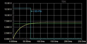
I thank for the scheme and the work schedule, what the constant green line being on level 6,5V and yellow, smoothly accruing to 7V means?Hi,
post circuit with lm339 solved a cut-off driver before uvlo intervent(PUP) when switch-Off psu.
at startup , also 65mS delay for enable driver not ensure that self-oscillator start.
Hi,
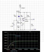
New Value for lm339 circuit.
you could try to connect "T2" with small capacitor on base for unbalance PWM at start-up.
P.S. high value fixed (Resistor) on SD to com, produce mistake signals driver at max power.
New Value for lm339 circuit.
you could try to connect "T2" with small capacitor on base for unbalance PWM at start-up.
P.S. high value fixed (Resistor) on SD to com, produce mistake signals driver at max power.
Attachments
Last edited:
Hi,Hi,
New Value for lm339 circuit.
you could try to connect "T2" with small capacitor on base for unbalance PWM at start-up.
P.S. high value fixed (Resistor) on SD to com, produce mistake signals driver at max power.
T2 I have cleaned definitively. A new variant of the scheme the final? For what you have added resistor R5 - 4,7K? On the schedule you have specified that a yellow line - PIN2, what is it? It is possible to see the schedule of work of a full cycle (inclusion/deenergizing), at use lm311 it is necessary to change any face values of components in the scheme?
Hi!
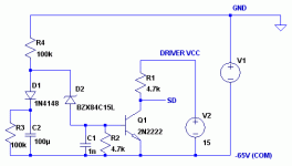
Here is my variant of driver shutdown circuit. This is very similar to my previous "deenergizing" scheme, but startup delay is added.
At startup Q1 is closed and SD signal is high (via R1). After C2 is charged to 15V (after about 3 seconds), Q1 will open and remove SD signal. The 3 seconds delay should be enough to allow high side to be charged, I think. Otherwise it will be needed to increase C2 to 220uF maybe.
When amp is switched off, Q1 will close again when power voltage is dropped to about 27-30 volts, and SD signal will be high again, providing 'smooth' deenergizing.
The C2 100uF cap should be at least 16V rated. D2 is any 15V Zener diode. Q1 can be 2N5551.")
I suggest you to build shutdown circuit on separate small board and then connect it to the main PCB to check it's functionality.
Here is my variant of driver shutdown circuit. This is very similar to my previous "deenergizing" scheme, but startup delay is added.
At startup Q1 is closed and SD signal is high (via R1). After C2 is charged to 15V (after about 3 seconds), Q1 will open and remove SD signal. The 3 seconds delay should be enough to allow high side to be charged, I think. Otherwise it will be needed to increase C2 to 220uF maybe.
When amp is switched off, Q1 will close again when power voltage is dropped to about 27-30 volts, and SD signal will be high again, providing 'smooth' deenergizing.
The C2 100uF cap should be at least 16V rated. D2 is any 15V Zener diode. Q1 can be 2N5551.
I suggest you to build shutdown circuit on separate small board and then connect it to the main PCB to check it's functionality.
Attachments
Last edited:
Hi,Hi!
Here is my variant of driver shutdown circuit. This is very similar to my previous "deenergizing" scheme, but startup delay is added.
At startup Q1 is closed and SD signal is high (via R1). After C2 is charged to 15V (after about 3 seconds), Q1 will open and remove SD signal. The 3 seconds delay should be enough to allow high side to be charged, I think. Otherwise it will be needed to increase C2 to 220uF maybe.
When amp is switched off, Q1 will close again when power voltage is dropped to about 27-30 volts, and SD signal will be high again, providing 'smooth' deenergizing.
The C2 100uF cap should be at least 16V rated. D2 is any 15V Zener diode. Q1 can be 2N5551.
I suggest you to build shutdown circuit on separate small board and then connect it to the main PCB to check it's functionality.
Thanks you for the scheme, has already drawn a PCB 4x4 сm
I will try. A question under the scheme: minus C2 goes on-65M (COM)? What power can be received from the given amplifier at a +/-65V main supply? In a filter I have condensers 2x47000mF.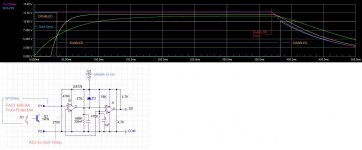
A question under the scheme: minus C2 goes on-65M (COM)?
Yes.
What power can be received from the given amplifier at a +/-65V main supply? In a filter I have condensers 2x47000mF.
With +/-65V supply you will get about 60Vp (peak voltage) at output.
Power is calculated in the following way: Vrms*Vrms/Rload
Vrms = Vp/sqrt(2) ~= Vp/1.4
So in your case with 4 Ohm load you will get:
Vrms ~= Vp/1.4 = 60/1.4 ~=43V
P = 43*43/4 ~= 462W
In BTL configuration Vp is doubled and for 4 Ohm we have:
Vrms ~= 120/1.4 ~= 85V
P = 85*85/4 ~= 1800W
These calculation do NOT account PSU sag under heavy load...
Last edited:
Very interesting decision, I plan to enter in the future protection of the amplifier against an overload, constant pressure on an exit and to add a limiter on an input. At present me interests elimination of two listed by me above problems (start from an entrance signal and a deenergizing impulse) whether two also are necessary for the decision of the given problems in your scheme opamp it is possible to simplify? I plan to use LM311, for it it is necessary to change something? You have told that not assured of scheme work 81bas if to you not difficultly that you could simulate its work as your scheme and show the schedule?Hi,
sorry for delay,I have many job.
81BAS. R3-C2 charge but...discharge?-- driver voltage drop before of +/-65v and create "PUP"....I think
I think is simple,lm339 is double comparator and component are SMD.
Also, create a fast-input for protections.
Functions is ok tested. also,if input protection used,this is good becouse Re-start with delay.
Ok, BTL configuration means bridge inclusion? I assume that capacities of the power transformer in 500W and capacities which I specified should suffice for capacity reception 460W on 4ohm at a Vcc +/-65V. To what maximum power you did amplifiers in class D?Yes.
With +/-65V supply you will get about 60Vp (peak voltage) at output.
Power is calculated in the following way: Vrms*Vrms/Rload
Vrms = Vp/sqrt(2) ~= Vp/1.4
So in your case with 4 Ohm load you will get:
Vrms ~= Vp/1.4 = 60/1.4 ~=43V
P = 43*43/4 ~= 462W
In BTL configuration Vp is doubled and for 4 Ohm we have:
Vrms ~= 120/1.4 ~= 85V
P = 85*85/4 ~= 1800W
These calculation do NOT account PSU sag under heavy load...
Ok, BTL configuration means bridge inclusion?
Yes. BTL = bridge tied load
I assume that capacities of the power transformer in 500W and capacities which I specified should suffice for capacity reception 460W on 4ohm at a Vcc +/-65V.
I think so too
To what maximum power you did amplifiers in class D?
This was a 300W carrier based class D amp with PSU sag compensation in modulator. But this is still not finished
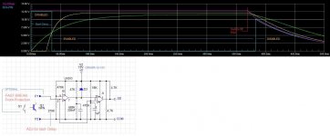
I am still experimenting with it... Hi All,
(Woow! .. I am using a big simulator for small problem)
now generates a small pulse immediately after EN-SD (it is important that happens later). for start oscillation.
the sequence of operation is reset at PSU-On and from ShuntDown protection.
small cap and parts, I think it occupies small space on the PCB.
to generate these 3 were logical, I can not think of another mode.(for now)
this is very simple.
can not use LM311.(lm393 is double comp)
Attachments
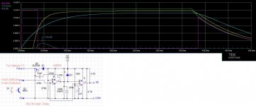
Hi,Hi!
Here is my variant of driver shutdown circuit. This is very similar to my previous "deenergizing" scheme, but startup delay is added.
At startup Q1 is closed and SD signal is high (via R1). After C2 is charged to 15V (after about 3 seconds), Q1 will open and remove SD signal. The 3 seconds delay should be enough to allow high side to be charged, I think. Otherwise it will be needed to increase C2 to 220uF maybe.
When amp is switched off, Q1 will close again when power voltage is dropped to about 27-30 volts, and SD signal will be high again, providing 'smooth' deenergizing.
The C2 100uF cap should be at least 16V rated. D2 is any 15V Zener diode. Q1 can be 2N5551.
I suggest you to build shutdown circuit on separate small board and then connect it to the main PCB to check it's functionality.
Has held testing of your scheme: has submitted two Vcc and has checked up potential on SD a conclusion, at startup/deenergizing the potential does not vary (the scheme does not work)
, I will try variant AP2 on a LM393.Hi,Hello Vigor,..To what extent is your amp?
you can proceed with LM393 circuit (4). Perfectly work, I can give you support when you're ready to adjust some value.
The amplifier works well, yet did not spend tests for the big capacity but I think that all will be ok, there was a problem with deenergizing... I Will try your scheme from a post #154, after experiments I will write about result.
Hi,
Has held testing of your scheme: has submitted two Vcc and has checked up potential on SD a conclusion, at startup/deenergizing the potential does not vary (the scheme does not work)
I have simulated it in LTSpice before posting it here, it works
Please, post your connections here, we will try to find the problem then...Hi,
Has held testing of your scheme: has submitted two Vcc and has checked up potential on SD a conclusion, at startup/deenergizing the potential does not vary (the scheme does not work)
Also, what means 'have submitted two Vcc' ? Did you connected it to GND as described too? How did you measured the 'potential on SD' ? Between GND and SD or between -65V and SD ?
- Status
- This old topic is closed. If you want to reopen this topic, contact a moderator using the "Report Post" button.
- Home
- Amplifiers
- Class D
- Self-oscillating class D amplifier