I would replace the DCB1 Buffer with a gain stage that accepts your source signals and has sufficient current to drive the cables feeding into your M2.hi Salas,
How can I add a gain stage to the DCB1 ? Seems like I need more gain in driving the M2.
Thanks
There are many gain stages described in this forum that are fully capable, without needing a DCB1 in front of them.
Hi here is a photo of the board I have. If it is not a DCB1 then what is it
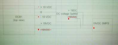
Keeping with the orientation in your photo the rail voltages pins to the right should be connected like in the annotated attachment. Someone obviously hacked off the shunt PSU section either to use it standalone for powering a Soekris etc. or could not fit the full board with sinks in an integrated build and split it or had another supply fitted already or had some other practical reason like that.
Attachments
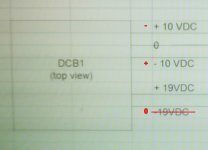
It can't be a DCB1.Hi I just managed to pick a finished DCB1 blue board nicely soldered up with 4 relay inputs. however the normally supplied power supply board has been removed (don't know why & didn't realize until after the purchase) Can I connect this little unit up to a Split rail voltage splitter (with adjustable voltages so I can achieve +/- 10 VDC) and feed the voltage splitter and second 18VDC requirement from a 19 VDC Laptop SMPS.
As per the attached photo as there is no indication of polarity on the board is my voltage assumptions on the attached sketch correct.
There was the original, then the Hypnotize and Mesmerize followed by the hotrodded.
All had the PSU integrated on the PCB.
The Hyp had one relay,
The Mes had 7 relays. Post5548 shows 7 relays with two left empty.
Last edited:
Hi Salas, Thanks for the correction info. Will the buffer work with this type of power configuration Cheers
It will rather work like this but not sure of quality or hum
Attachments

I have not heard a B1 so can't compare directly.
I am surprised that the B1 is being reported as audibly inferior to the DCB1 since they are essentially the same circuit, a jFET Follower with CCS loading.
Both the DCB1 and the B1 will have a DC blocking capacitor before and after the Buffer stage, unless some considerable "other circuits" are added to minimise the effects of DC getting to the speaker load.
none.
Thanks, Andrew. I thought I read somewhere in the thread that you need to change a resistor value to accommodate the 50k pot.
I don't think so. It just feeds the Buffer with a slightly higher source impedance and that will affect the accidental RF filter created by the input capacitance of the jFET.
Better to use a lower value vol pot and add proper RF attenuation filtering that does not change with signal voltage.
Better to use a lower value vol pot and add proper RF attenuation filtering that does not change with signal voltage.
I thought I read somewhere in the thread that you need to change a resistor value to accommodate the 50k pot.
We used to put 560k instead of 220k input to ground resistor for 50k pot just to keep the ratios same as with the standard 20K pot but its not really significant. We usually preferred the 20K pot 220k arrangement slightly better subjectively.
- Home
- Source & Line
- Analog Line Level
- Salas hotrodded blue DCB1 build