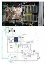
There's only one earth wire at the IEC and there are two connections to it, ie. the chassis and the PSU ground. Somewhere along the way, if the the PSU ground is connected to the thermistor, the chassis connection is bound to come into contact with the thermistor. I don't think there's a way to avoid this.
check here ..
https://www.youtube.com/watch?v=m9YBOwVMos4
https://www.youtube.com/watch?v=InJhgwmj2So
Br Walter
https://www.youtube.com/watch?v=m9YBOwVMos4
https://www.youtube.com/watch?v=InJhgwmj2So
Br Walter
Hi Andrew, Thanks but if I connect the Mains PE to the chassis then where do I connect the PSU ground to? Could you be kind enough to sketch out the diagram?
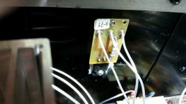
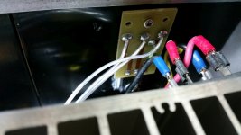
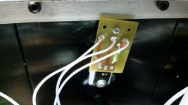
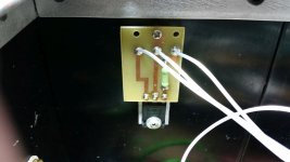
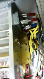
safety gnd from IEC socket directly to chassis
audio ground (central point) connected to chassis via 10R to 15R NTC
say CL60
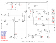
Does Q3 and Q4 needs to be matched?
no ; they're having completely different role
upper one is for programming current in Aleph CCS , lower one is peak/safety current limiter
Thanks ZM and AndrewT. I appreciate both of your help very much. Does the attached 'diagram5' looks right for the PE connection? Also, what is the likely problem for the big difference of voltage across the source resistor if the mosfets are matched (aj measure2)?
Attachments
Thanks ZM and AndrewT. I appreciate both of your help very much. Does the attached 'diagram5' looks right for the PE connection? Also, what is the likely problem for the big difference of voltage across the source resistor if the mosfets are matched (aj measure2)?
look (red !!) where is difference , comparing to your drawing
if source resistors are close enough in value (5% usual tolerance) , then mosfets aren't matched
you need to have two matched pairs - one pair going in upper half , second pair going in lower half
edit : it seems Q8 is bad neighbor
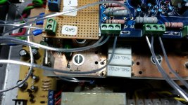
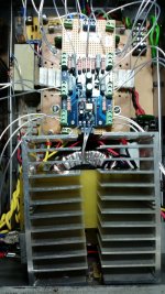
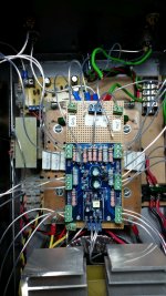
During testing after swapping the mosfets, I accidentally touch an output resistor (between a source resistor and an output resistor) and damn. Now I have a source resistor giving a 3.0v reading (this is the extra mosfet that i add in, which is the R19A). The Z1 remains at 8.9 and R8 remains at 8.4v. R27 remains at 4.1v. The readings between Gate and Source of the mosfets are between 0.4 to 0.45v. I have checked the mosfets and they remain good and I have even replaced Q3 and Q4. How now?
Last edited:
look (red !!) where is difference , comparing to your drawing
if source resistors are close enough in value (5% usual tolerance) , then mosfets aren't matched
you need to have two matched pairs - one pair going in upper half , second pair going in lower half
edit : it seems Q8 is bad neighbor
When you said 'upper and lower half' you mean, Q5 and Q6 to be matched and then Q7 and Q8 to be matched, right? Q5 and Q6 are the current source while Q7 and Q8 are the output mosfets, correct?
Last edited:
During testing after swapping the mosfets, I accidentally touch an output resistor (between a source resistor and an output resistor) and damn. Now I have a source resistor giving a 3.0v reading (this is the extra mosfet that i add in, which is the R19A). The Z1 remains at 8.9 and R8 remains at 8.4v. R27 remains at 4.1v. The readings between Gate and Source of the mosfets are between 0.4 to 0.45v. I have checked the mosfets and they remain good and I have even replaced Q3 and Q4. How now?
if in doubt - replace ....... then think
price of learning process

When you said 'upper and lower half' you mean, Q5 and Q6 to be matched and then Q7 and Q8 to be matched, right? Q5 and Q6 are the current source while Q7 and Q8 are the output mosfets, correct?
exactly
I have changed all components to new ones except for all the source resistors but the problem persists. I don't think the problem is with the board. I suspect it's the power supply. Now, the power supply is at 54V. Previously it was at 56v, I wonder where did the 2v go? and the problem is exactly the same as before, the dc offset went up to 80mv and now it is at 100mV. The additional 19A source resistor goes up even higher at 0.900v but the R19 remains at 0.534v no matter how i swapped them.
Last edited:
mains power at 240v.
Attachments
-
 20140820_204120.jpg193.5 KB · Views: 38
 -
 20140820_204105.jpg154.8 KB · Views: 37
 -
 20140820_204048.jpg126.3 KB · Views: 34
 -
 20140820_204033.jpg124.6 KB · Views: 38
 -
 20140820_204022.jpg130.9 KB · Views: 63
 -
 20140820_204015.jpg118.4 KB · Views: 74
 -
 20140820_203956.jpg336.9 KB · Views: 74
 -
 20140820_203944.jpg485.9 KB · Views: 79
 -
 20140820_203937.jpg499.2 KB · Views: 79
 -
 20140820_204130.jpg144.7 KB · Views: 36
- Status
- This old topic is closed. If you want to reopen this topic, contact a moderator using the "Report Post" button.
- Home
- Amplifiers
- Pass Labs
- Rising DC Offset