Those look fine beta's might be a little high, just test for gm at the current you want to run at.
I've been to busy to go to the next step, but I'll try to post a block diagram. The basic circuit worked fine as headphone driver with the buffers, but I have not tried my output error correction idea yet.
I've been to busy to go to the next step, but I'll try to post a block diagram. The basic circuit worked fine as headphone driver with the buffers, but I have not tried my output error correction idea yet.
nikwal said:Yeah, build it...
I've made and built this below some time ago.. It aint all that bad.. The principle is good and I'm very pleased with the sound..
http://www.diyaudio.com/forums/showthread.php?s=&threadid=130475
I didn't read your whole thread but connecting all four caps that way misses the whole point. Now the compensation capacitance is also bootstrapped away. This way the caps only appear in the common mode path. The circuit could fine stability from another path anyway but not the intended one.
Ok, I said that I would not post on this again until I actually built one and tried it out. So I did. This is a work in progress and I’m sure a couple of warts will show up and there is some tweaking to do. Hopefully I’m not missing anything fatal.
I'm in a sharing mood today. You've still got those 2k resistors loading the LTP's to kill that gain and tame the sensitivity to DC imbalance.
How much supply rail head room would you be willing to burn?
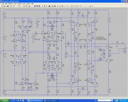
Attached is a (somewhat) simplified and scaled-down front-end schemaic of what I've finally settled on for my slightly OTT 100A / 1200W idle house heater.
I solved the issue of low resistance LTP loads and maintained very good DC balance with two tricks - capacitive coupling at the VAS transistor emitters and high voltage DC rails. Although a pair of trimpots are still required at the LTP emitters to null out the DC offset between the collectors.
Ta da!
The linearity is an order of magnitude better.
Attachments
Last edited:
Gosh I can be such a dummy!
The DC gain kill on the VAS is only mildly effective - it's the input stage where the DC gain needs to be killed with capacitive coupling (obviously - duh!)
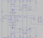
Here it is. The LTP's have a DC gain of unity, so the input offset/imbalance problem is solved, but the cap-coupled degeneration ensures high AC gain - much better than a 1K or a 2k gain kill resistor collector-collector!
Ta da!
The DC gain kill on the VAS is only mildly effective - it's the input stage where the DC gain needs to be killed with capacitive coupling (obviously - duh!)
Here it is. The LTP's have a DC gain of unity, so the input offset/imbalance problem is solved, but the cap-coupled degeneration ensures high AC gain - much better than a 1K or a 2k gain kill resistor collector-collector!
Ta da!
Attachments
MKIII
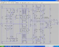
Turns out that AC coupling (DC gain-kill) of the emitter degeneration will be required for both the LTP and the VAS I'm trying for an acceptable degree of VAS imbalance with worse case 0.2% error in the resistors (will buy 0.1% types). Some degree of DC gain is still required though, for adequate servoing of the DC operating point.
I'm getting there............
Turns out that AC coupling (DC gain-kill) of the emitter degeneration will be required for both the LTP and the VAS
I'm trying for an acceptable degree of VAS imbalance with worse case 0.2% error in the resistors (will buy 0.1% types). Some degree of DC gain is still required though, for adequate servoing of the DC operating point.I'm getting there............
Attachments
Last edited:
- Status
- This old topic is closed. If you want to reopen this topic, contact a moderator using the "Report Post" button.