Ouroboros said:A simple SPICE simulation (such as the attached TINA schematic) will show that the performance using a voltage-amplifer or a transconductance amplifier for the Class-A stage makes very little difference to the measured performance.
I have used a VCVS and a VCCS for the class-A stages so that it's very easy to alter the voltage or current gain of the stage to perform the simulation runs.
I use two QUAD 405s with the original amplifier boards replaced my my own current-dumping design, and still think the this principle is still up there with the best when it comes to amplifier topologies. Peter Walker was a very bright guy to come up with the idea. It's just a pity that the original implementation was so poor.
Well...the analysis by Hevreng is quite simple and straightforward and above it is correct. If whatever model does not yield the conclusions and predictions therein then it is just ..wrong.
No the effect of G0 and hence Z0 and unity gain frequency of class A is significant and cannot be neglected.
This is just about a class A without integrated opamp without differential input and without current sources so G0 will be low
and Z0 will be considerably high. Then if Z2 is a capacitor or an RC combination it is impossible to have a frequency- independent error compensation.
Notwithstanding the current dumping is an excellent implementation of error feedforward correction at least on paper.
However the question is whether one can achieve pretty much the same subjective quality with simple nested negative feedback. Or even better. That is however pointless as subjective impression is not possible to objectify it is a quality not a quantity.
Lumba Ogir said:hahfran,
2SK135/2SJ50 are sonically superior to anything else, please without hesitation look at this previously suggested suitable design equipped with genuine single-ended input and evenly genuine CFP output stage.
(Another option is disposing of them for many bucks).
http://www.diyaudio.com/forums/atta...tamp=1225821617
Lumba the link is dead. I have just two pairs of these old FETs but I would need at least six. Since the project should be done in a few weeks from now I'd prefer a prestage driver for which I have a proven PCB layout. I would not mount the output trans and the drivers on the same PCB. Rather the voltage to current stage should be considerably far off the predriver board to avoid
influence of EM fields.
hahfran,
you don`t need PCB for the output stages, just place master and slave in close proximity to each other but thermally isolated. This is important.
The prestage section should have much higher voltage power supply.

you don`t need PCB for the output stages, just place master and slave in close proximity to each other but thermally isolated. This is important.
The prestage section should have much higher voltage power supply.
Me too.I would need at least six.
Two methods
the simplest two channel scope in difference mode shows after calibration the difference of out and in
more sensitive the difference of input and feedback signal ( or error correction signal ) at the error take off point as described by Sandman. The inverting input is a virtual ground. This does not work so good in my preamp possibly because it has very low G0.
The first method gives in my case more plausible results if a software spectrum analyzer is used combined with the scope.
The analyzer is however not too trustworthy.
Nevertheless with a discrete prestage class A with low open loop gain G0 considerable output impedance Zo the crossover of the Quad303 rebuild is about the same as of current dumping however it requires no trimming for minimum procedure of passive bridge components as there are none. So it is an open race yet.
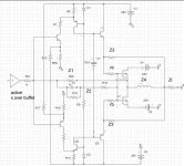
Current dumping amp Scottish version
I don't know whether Scotsmen are thrifty...rather I think they use resources effectively. Anyway this current dumping amp gets along with 8 active transistors plus 1 Vbe multiplier. After all no transistors
create no signal errors. A Sorites paradox, I know.
Diodes are green LEds forward voltage about 2.3 Volts.
The class A driver has a high open loop gain Go the common collector driver provides low Zo thus that rb=Zo/Go*(1+Z2/R1+Z2/Ri) can be implemented as the RC given by a real rb and the Cgs of the FETs.
Z2 is implemented as R18 C1 R19.
The class A is very fast this topology does not require Miller capacitors.
This amp is intended only as driver for active speakers so the current feedback to inverting input which is a virtual ground is not a disadvantage because the input is tied to the output of a buffer of the active crossover with a known output impedance.
The circuit schematic looks promising as for now I don't have an idea whether it will work.
Attachments
hahfran,
if you ask me (you probably don`t) I like this one more than that in post #142, despite the complementary input structure.
if you ask me (you probably don`t) I like this one more than that in post #142, despite the complementary input structure.
No paradox or contradiction here, simplicity is a good principle, the tricky part is determining its level. (I would omit Q1/Q3).After all no transistors create no signal errors. A Sorites paradox, I know.
Lumba
Q1 Q3 cannot be omitted this common collector push pull stage provides both high Go and low Zo further the input cascade quiescent current must be set with respect to high fT and low noise. That is for
epiplanar BJT met at about 3mA to 5 mA. The quiescent current of Q1 Q3 is set to 100 mA .
Anyway I am not sure whether it will work.
LQ 405 .....same schematic ...another PCB
Hi,
PCB for Quad 405 with lateral mosfet K1058 and j162 , http://i39.tinypic.com/zvbd3n.jpg .
regards alex mm
Hi,
PCB for Quad 405 with lateral mosfet K1058 and j162 , http://i39.tinypic.com/zvbd3n.jpg .
regards alex mm
Re: Current dumping amp Scottish version
Well it works however the calculation according to theory of Z1 thru Z4 does not yield optimum results in practice some fine tuning is
required. But primarily results are promising the current dumping amp can be made pretty fast so far I've achieved a rise time of
15 V/usec. Crossover distortion can be shifted to 8 kHz and up.
Unfortunately BUZ900 BUZ906 became unavailable I have just one pair for testing. This device has a low junction to case resistance
so I could get 50 Watts in 8 ohms with present heatsinks these cannot be made any bigger due to volume restrictions in the speaker enclosure.
hahfran said:I don't know whether Scotsmen are thrifty...rather I think they use resources effectively. Anyway this current dumping amp gets along with 8 active transistors plus 1 Vbe multiplier. After all no transistors
create no signal errors. A Sorites paradox, I know.
Diodes are green LEds forward voltage about 2.3 Volts.
The class A driver has a high open loop gain Go the common collector driver provides low Zo thus that rb=Zo/Go*(1+Z2/R1+Z2/Ri) can be implemented as the RC given by a real rb and the Cgs of the FETs.
Z2 is implemented as R18 C1 R19.
The class A is very fast this topology does not require Miller capacitors.
This amp is intended only as driver for active speakers so the current feedback to inverting input which is a virtual ground is not a disadvantage because the input is tied to the output of a buffer of the active crossover with a known output impedance.
The circuit schematic looks promising as for now I don't have an idea whether it will work.
Well it works however the calculation according to theory of Z1 thru Z4 does not yield optimum results in practice some fine tuning is
required. But primarily results are promising the current dumping amp can be made pretty fast so far I've achieved a rise time of
15 V/usec. Crossover distortion can be shifted to 8 kHz and up.
Unfortunately BUZ900 BUZ906 became unavailable I have just one pair for testing. This device has a low junction to case resistance
so I could get 50 Watts in 8 ohms with present heatsinks these cannot be made any bigger due to volume restrictions in the speaker enclosure.
more pic ..... LQ 405
Hi ,
link to another pic http://i40.tinypic.com/2s198k8.jpg
regards alex mm.
Marry Christmas to all !
Hi ,
link to another pic
http://i40.tinypic.com/2s198k8.jpg regards alex mm.
Marry Christmas to all !
silk screen .......
Hi,
no, it's gest silk screen , air coil inductor mounted now http://i40.tinypic.com/11r3wnn.jpg
Marry Christmas ! alex mm
Hi,
no, it's gest silk screen , air coil inductor mounted now
http://i40.tinypic.com/11r3wnn.jpg Marry Christmas ! alex mm
The difficulty with DIY a current dumping amp is indeed the inductor.
If computation ( it will yield, if correctly done, optimum values for
the 4 bridge elements ) results a particular inductivity L then how would one make an inductor which has, amongst other properties,
the inductivity L?
The most exact approximation is a straight (nowhere bent or curved) wire. That however would turn out a bit long, about 3.05 meters for 3uH.
The best approximation of a straight wire is a spiral. However there is exactly one straight wire but as many as you please spirals.
A cylindrical coil inductor is not well predictable in terms of inductivity
by approximate formula one has to expect deviations in the range of 20% + or - . It must further be expected that due to electromagnetic
forces the inductivity will depend on the current value.
So I am quite suspicious about enthusiastic reports about DIY current dumping amps if it is nowhere mentioned how the inductivity is physically realized.
I've had very good results with the powered iron mix toroids wound with several parallel windings of 24 gauge wire. The moly perm cores that Magnetics Inc sells work well too but are a little harder to procure, although they will usually give you a sample piece for no charge.
I have always been wary of ferrite cores as they saturate pretty readily with non symetrical waveforms.
Air core inductors are a possibility too, but probably have a higher series resistance.
You can buy a DMM with an inductance reading relatively inexpensively. They measure capcitors too, so they come in handy.
Sure inexpensive DMMs come with inductance and capacitance range..
However from the current dumping theory it is evident that the insensitivity to power transistor properties comes at the price of
"infinite" accuracy of the passive bridge components.
( As well as "infinite" gain of the class A)
Only a printed inductor is reproducible in terms of inductance.
So one has to do it only once - it is the same difference as between
hand writing and typing ASCII code for characters. To decode hand written symbols you need a powerful computer brain or such but any simple logic gate can decode ASCII coded bytes....
Whenever I am doing some home improvement my wife books a hotel appartment in advance in case the house has to be evacuated or worst case to be rebuild. I could not wind up any two similar inductors.
So I have to do some thinking to avoid flop.
- Home
- Amplifiers
- Solid State
- QUASAR a reborn design