Will get back to you.
I agree with your finding Ingenius, this is a very complex amplifier. Besides, there is not much phase margin at 0dB and I think the amp will be unstable when driving capacitive loads.
Kind regards
Nico
Mr Nico Ras, could you give me some more details about this :
"Besides, there is not much phase margin at 0dB and I think the amp will be unstable when driving capacitive loads."?
I want to find out more, and if it is something to worry about, how can we change this?
thank you,
sergiu
"Besides, there is not much phase margin at 0dB and I think the amp will be unstable when driving capacitive loads."?
I want to find out more, and if it is something to worry about, how can we change this?
thank you,
sergiu
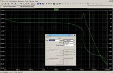
a few corrections
stability looks correct
distorsion 1kHz look correct
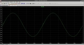
sinus 20kHz shows a crossover glitch
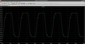
square wave 100kHz shows the output devices switching
lateral mosfets as output devices may be more appropriate
stability looks correct
distorsion 1kHz look correct
sinus 20kHz shows a crossover glitch
square wave 100kHz shows the output devices switching
lateral mosfets as output devices may be more appropriate
Attachments
Last edited:
Hi Sergui, firstly this is an informal site and Mr, is not necessary - we are all members of the same club ")
What I meant is that one needs to design so not have a phase inversion while the amp still has gain.
It looks as if the amp at >0dB gain the phase shift is -180 degree and that into a pure resistive load. Should some reactive load be present it would most certainly cause oscillation at a high frequency.
It suggests in some early threads that one should aim for at least 50 degrees margin at 0dB, in other words a phase shift of less than -130 degrees.
It is not possible to always see this oscillation spike in a frequency/phase response simulation as the gain curve masks it.
Nico
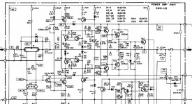
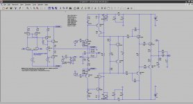
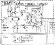
I saw you trying to reinvent the wheel with a True Symmetry amplifier, which is a topology dating back from december 1973 (Motorola publication in Radio-Electronics), made popular by Erno Borbely (Hafler DH-200 in 1978) and prof. Leach as soon as 1976 (the Leach amp).mr steph, what is the purpose of the stage from bellow the input stage (wich looks the same as the input one) on post 45?
I guessed that you want a zero capacitor design. No capactor at the input. No capacitor in the feedback network.
I saw the many potentiometers in your design, the complexity of the input stage, and I guessed that you wanted to replace the differential BJTs by differential FETs.
Then comes the extra problem : you need to cascode the FETs for protecting them from the relatively high voltage supply rails. If you implement all this you get a monster, many many parts, you need matched parts, trimmers, all sources of problems.
Actually, 10 years after Motorola showed the True Symmetry amplifier, Mr Kuroda had the idea to use a TL071 FET opamp as front-end for a True Symmetry amplifier, in 1983. He did the amp in 1983, it worked, and it got published.
Mr Kuroda uses the FET opamp as voltage-to-current converter. Basically what he is doing is to connect the output of the opamp to the ground, through a 150 ohm resistor. You then need to observe that the signal used by the power amp VAS is the current supplied to the opamp, by the -V and +V pins of the opamp.
There were stability issues. In order to get a stable amplifier, Mr Kuroda added a dedicated voltage feedback going from the power amp output, to the opamp output. Such feedback forces the opamp to work with a certain voltage swing at its output. Such voltage swing helps the opamp sensing what's going on at the power amp output, much faster than the relatively slow differential input of the opamp. If there is something wrong at the power amplifier output, there is an extra-voltage showing at the output of the opamp, which forces the opamp to absorbe it, and such absorbsion causes a variation in the -V and +V pins of the opamp.
So effectively, in a Kuroda topology, you get two embedded systems : the slow system which is encompassing the differential input of the opamp, and the fast system which only consists of the opamp output transistors.
Most people fail getting a Kuroda working proprely, because they don't understand the importance of having the fast loop correctly setup with the correct resistor values. You also need to manage the slow loop, like using a compensaton capacitor : 33pF to 68pF maybe.
Usually, there is a Miller capacitor in the VAS. In a True Symmetry amplifier, there are two complementary VAS operating in parallel. What I have found is that if you setup the fast loop in an optimal way, the Miller capacitor that you may need to add in the VAS remains minimal, which is a very good way for maximizing the slew rates.
A Kuroda amplifier retains some positive aspects of a current feedback amplifier. When the amplifier needs to deliver a fast slew rate, quickly charging all parasitic capacitors, the VAS can deliver more than twice the VAS idle current. You need to note the current limitation that's implemented in the V- V+ supply pin of the opamp. If such current limitation is not in place, the current sinked by the V- V+ pins can exceed 10 times the quiescent supply of the opamp. Which means that the VAS will deliver 10 times the VAS quiescent current. This can be too much indeed.
The latest trend regarding Kuroda amplifiers is to configure the VAS as a precision current mirror with a unity current transfer functon.
A VAS normally operates at a current which is bigger than an opamp quiescent current. We thus use multiple VAS in parallel. This way, high voltage transistors having very low reverse capacitance can be used in the VAS, with low base charge storage and a Ft of at least 300 MHz.
Let's take an example. Say the FET opamp has a quiescent supply of 3mA.
Say there are 4 VAS in parallel, each with a unity transfer function.
The VAS total quiescent current will be 12mA.
A non-Kuroda amplifier would only be able to drive the VAS to 24mA, twice the quiescent.
A Kuroda can get the VAS delivering 10 times the quiescent, so 120mA, if no current limit is defined in the V- V+ supply pins of the opamp.
A wise choice is to limit the opamp supply to 12mA, which means 48mA max in the VAS, meaning twice the slew rate.
A more agressive choice is to limit the opamp supply at 18mA, which means 72mA max in the VAS, meaning three times the slew rate. Cascoding the VAS, one cascode per transistor, may be needed for not exceeding the dissipation in the current mirrors.
Hope you will enjoy the Kuroda.
Best regards,
Steph
Last edited:
Nico Ras, thank you for accepting me in the club..
Thanks for the enlightenment, i am searching for a database for my lt spice program wich includes some more transistors, and try to simulate this reactive load, what i meant is that i will try to simulate the schematic with different frequencies on the input and try to increase in the same time the load (from 8 to 12 to 16, and up to 46 ohms)..
sergiu
PS: i'm still studying the lt spice program..
Hi ,
Pioneer non-switching trick is a very good idea. Look this Pioneer A-5 | Owners Manual, Service Manual, Schematics, Free Download | HiFi Engine
Yamaha hyperbolic amplifier is same circuit.......not identicaly .
That can be disadvantages to this method?
It is no longer used in modern diagrams?
Pioneer non-switching trick is a very good idea. Look this Pioneer A-5 | Owners Manual, Service Manual, Schematics, Free Download | HiFi Engine
Yamaha hyperbolic amplifier is same circuit.......not identicaly .
That can be disadvantages to this method?
It is no longer used in modern diagrams?
Attachments
Last edited:
I think it is no longer used in modern amplifiers because if you use lateral mosfets as output devices, most crossover problems are gone. Be carefull when simulating the Pioneer non-switching arrangement using LTspiceIV. This is a difficult circuit. Some time ago I have tried a simulation. The results were not convincing and LTspiceIV had convergence problems. I needed to operate at a bias current of about 250mA for guaranteeing the non-switching feature at low and medium power levels. I never managed to keep the system non-switching at high power levels. The method is very sensitive to the BJT LTspiceIV model used. Have you looked to the Sansui non-switching circuit also ?Hi, Pioneer non-switching trick is a very good idea.
Why is it no longer used in modern diagrams?
I think it is no longer used in modern amplifiers because if you use lateral mosfets as output devices, most crossover problems are gone. Be carefull when simulating the Pioneer non-switching arrangement using LTspiceIV. This is a difficult circuit. Some time ago I have tried a simulation. The results were not convincing and LTspiceIV had convergence problems. I needed to operate at a bias current of about 250mA for guaranteeing the non-switching feature at low and medium power levels. I never managed to keep the system non-switching at high power levels. The method is very sensitive to the BJT LTspiceIV model used. Have you looked to the Sansui non-switching circuit also ?
Please , can you tell me what model of amplifier used SANSUI non-switching technology ?
JVC, Pioneer, Sansui non-switching schematics : read the thread on diyAudio : http://www.diyaudio.com/forums/solid-state/162559-new-class-super-non-switching-need-revival.htmlI found only schematic to amplifier B77 SANSUI non switching technology , unfortunately is of poor quality and do not see the values of components , please help .......
Do you know the "Renardson Ultralinear" ? Read the thread on diyAudio : http://www.diyaudio.com/forums/solid-state/163231-class-ab-soft-non-switching-2.html
Read also this about the "Renardson Ultralinear" : http://www.linearaudio.nl/Miscellaneous/renardson new class B.pdf
Last edited:
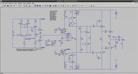
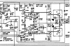
Now I understand what you say ........... compensation will be very effective by adjusting ( increasing ) values of R42 / R49 + C 20 / C21 and R56 / R57, analyzing the output capacitive load recommended 2 microfarads. Simulation is available for your 2SA / 2SC not for type MJ / MJL....................?
I hope you change wrong values simulated from the first scheme, as recommended by SORINSISTEM1 were some errors ,
Thanks in advance for your interest, Victor
I hope you change wrong values simulated from the first scheme, as recommended by SORINSISTEM1 were some errors ,
Please attach files with graphics amplitude frequency, phase error and distortion etc , in jpg format , not LTspiceFor a correct simulation, please make the following changes: eliminate C7 and C8; R9 and R10 resistors are 1Kohm, R50, R51, R42, R49 = 5.6 R, R15 = 120k, please eliminate from the schematic the circuit JP1, JP2 (because we dont need them),and connect correctly R51 between the C22, C23 and C24, C25 capacitors... DZ3 and DZ4 are rated at 3.9 volts.
Thanks in advance for your interest, Victor
Last edited:
- Status
- This old topic is closed. If you want to reopen this topic, contact a moderator using the "Report Post" button.
- Home
- Amplifiers
- Solid State
- PSA 150 S (pure sound amplifier)---help needed