I wish I could work with LTspice as well as you do gootee, you seem a pro at itI've always worked with MultiSim and like to think I'm pretty proficient at using it, but what you do with LTspace makes my sessions look like child's play.
Thanks but I am not really that great at it. I used it every day for a few years but there are many advanced methods that I never learned to use. There are some people I used to talk with, from the LT-Spice users group at yahoogroups.com, who are ten times or maybe a hundred times more-knowledgable about it than I am. There are many here at diyaudio, too, who are true LT-Spice "power users".
I am still playing with the power supply simulation setup and will post it soon, so everyone else can play with it too.
Not exactly on topic, but I'm gung ho about worrying about everything, including RF interference effects. This piece is a pretty impresssive rundown on the sort of things that can be considered, and note that I have not digested it properly myself. But it should yield some ideas: PCB DESIGN TECHNIQUES FOR LOWEST-COST EMC COMPLIANCEHi guys,
Here is an example of some of the ideas discussed on this thread regarding local decoupling. I'm working on this F5 layout since I might be doing a second amp. This layout is not finished and there are several errors in it so this is just to show one way to accomplish the local decoupling using 47u + 220u + 2200 or 4,700u and would like to hear your comments.
Frank
Hi Guys,
I am back from my week long trip and I have read all the posts since I left. Tom, your contributions has been priceless. I thank you sincerely.
If everyone capable, had a go at your simulation I can pretty much say that we may reach some conclusions and applicable rules of thumb, or rather a guideline to the requirements of a power supply for an audio application.
All,
Attached are the four files for a very simple power supply test-simulation. I have much-more-detailed ones that I will upload soon. But this one will get everyone started.
Just copy all four of the files into your LT-Spice folder. (In Internet Explorer, just right-click on each one and select "Save Target As".)
Change the names of two of them, to remove the ".txt" from the end of the file names.
(LT-Spice can be downloaded for free from linear.com .)
Then, from LT-Spice, open the schematic file named PSU_Test_1.asc.
Then click the "Run" (running man) button, to start the simulation. It is currently set to run for 150 ms of operation.
This one doesn't model most of the conductor parasitics; only the power and ground rails. I will soon upload one or two that also model most of the component interconnections' conductors' parasitics.
This one does include a power transformer model, which can be changed, later, if you follow the built-in instructions and measure a real transformer. (Right now, it models a little Hammond 120VA 25-Volt 4.8A toroid.) The power transformer model is probably only good for single primary and single secondary transformers, but seems to also work for dual/dual transformers, if primaries are paralleled and secondaries are paralleled, as this one was. There is a PDF link on the transformer schematic that might enable someone to extend the model for more secondaries.
Cheers,
Tom
Attachments
Last edited:
Hi guys,
Here is an example of some of the ideas discussed on this thread regarding local decoupling. I'm working on this F5 layout since I might be doing a second amp. This layout is not finished and there are several errors in it so this is just to show one way to accomplish the local decoupling using 47u + 220u + 2200 or 4,700u and would like to hear your comments.
On the running amp I have decoupling done with 4,700u plus a film 0.1u which I will replace in the future with a 220u and see if I can here differences. The PSU is quite heavy with a couple of 800VA trafos and a CLC filter feeding both channels.
The new amp will have only one trafo and a similar CLC PSU
What do you think?
Cheers, Tony
Tony,
A schematic would be great.
What are the R11 values? And what do they do? Damping?
Wow, are you actually bringing separate power and ground to each decoupling cap?! Coool!!
And two parallel paths from there to the device! Nice!
I wish there was some way to get the decoupling caps closer to the device. But the parallel paths will help mitigate that, a lot.
Are you sure that your high-current traces are wide-enough?
Is there a ground plane that you didn't show? Otherwise I would worry that the "signal in" and "signal ground in" are separated as they are. You need a separate ground plane for signal ground, for that area, to stay over or under the signal in. Otherwise those two will have some "enclosed loop area" and will be a hum and noise antenna. Alternatively, you could try keeping those two very close together, everywhere.
It looks great, overall!
Cheers,
Tom
Last edited:
Thanks for putting that up, Tom ...All,
Attached are the four files for a very simple power supply test-simulation. I have much-more-detailed ones that I will upload soon. But this one will get everyone started.
Before I get too serious with it, I would just query the decoupling cap characteristics -- some of them don't match the typical parasitic characteristics of cap's I've seen, in particular C8, C16 and their matching cousins. Did you have any particular brand or style of devices here?
Cheers,
Frank
Thanks for putting that up, Tom ...
Before I get too serious with it, I would just query the decoupling cap characteristics -- some of them don't match the typical parasitic characteristics of cap's I've seen, in particular C8, C16 and their matching cousins. Did you have any particular brand or style of devices here?
Cheers,
Frank
Frank,
OK, this is the quick-and-dirty one that I threw together to buy me some time to keep working on the "real" ones for a little longer. <smile>
First, let me say that the cap values that I have in that model are not in any way what I think should be in there, to make a good power supply. Those are for people to experiment with.
(From what I'm seeing so far, I'd want at least 50-60000 uF divided among several reservoir caps per rail, with small Rs in series in between them, and at least 10000 uF of decoupling per side.)
Anyway, C16 and C9, the 1 uF decoupling caps, were kind of left in there like that, accidentally. Just right-click on them and change them to have the characteristics of a nice film cap.
What's wrong with C8 and C10? They are supposed to be 220 uF electrolytics. I have their ESR set to 0.603 Ohms and their parasitic inductances set to 2 nH. The 2 nH should probably be a nH fo each mm of lead-spacing so maybe 2 nH is slightly too small. (If you have data from real capacitors, or from manufacturers, we could definitely use some of that, about now.) Oh, OK. I looked at some stuff I did a few years ago and I was using 9 nH for 220 uF caps.
I probably should have left everything how it was in an earlier version, but I started playing around and then uploaded it a while later, without checking everything again. Originally, I had a 0.1 uF cap for each rail, that was supposed to stay there and not be removed or changed, to ensure that the simulation would stay running. Then I moved that where the 1 uF is now. Then I changed it to 1 uF as an experiment. Then I added the 220 uF. Sorry, it's been a long weekend.
Tom
Edit: If you look at the first plot pane, which has the rail currents and the decoupling cap currents, you can literally SEE the power supply rejection happening, and (almost) all of the ripple "canceling out".
It helps a lot if you maximize the plot window. Then you should also "ZOOM IN" by dragging a rectangle around the area you want to zoom. First, zoom to just a couple of cycles. (NOTE! To UNZOOM, click the magnifying glass that has an "X" through it. That is also useful to make the schematic fill its window again, whenever it doesn't. It may be the most-important button on the whole screen.)
Last edited:
Tom, I'm just a fussy bloke ...!
"Inductance is the equivalent series inductance, and it is rel-
atively independent of both frequency and temperature.
Typical values range from 2 to 8 nH for SMT types, 10 nH
to 30 nH for radial-leaded types, 20 to 50 nH for screw-ter-
minal types, and up to 200 nH for axial-leaded types.
These low values are achieved by tab location and intrinsic,
low inductance of the dielectric contact geometry. The
capacitor element has typical inductance of less than 2 nH."
So it's all about the geometry, there's no easy look up table for such things, you have to nominate the precise unit you're going to use to get a reasonable figure.
With regard to real data, I have dozens and dozens of PDFs from manufacturers and others that I've accumulated over the years; this allows me to to do pretty good guesstimates of values, especially knowing what the curves of the impedance vs. frequency should look like for a certain cap type. Unfortunately, no beautiful reference table or spreadsheet that gives me spot on numbers -- something for another day ...
With LTspice, one thing that really bugs me, because I like the individual tabs to be maximised on the screen to get as much detail showing as possible, is that if you then swap between the plot and schematic that the zoom level of the schematic is lost. This was driving me nuts, until I found a workaround: zoom right, right back and stick a couple of dummy grounds on the diagonals. This is probably totally irrelevant to 99.9% of users, but works a treat for me.
Frank
ESR is about right, but ESL should be about 16hH ...Anyway, C16 and C9, the 1 uF decoupling caps, were kind of left in there like that, accidentally. Just right-click on them and change them to have the characteristics of a nice film cap.
Even that might be a bit low -- from a Cornell Dubulier PDF:What's wrong with C8 and C10? They are supposed to be 220 uF electrolytics. I have their ESR set to 0.603 Ohms and their parasitic inductances set to 2 nH. The 2 nH should probably be a nH fo each mm of lead-spacing so maybe 2 nH is slightly too small. (If you have data from real capacitors, or from manufacturers, we could definitely use some of that, about now.) Oh, OK. I looked at some stuff I did a few years ago and I was using 9 nH for 220 uF caps.
"Inductance is the equivalent series inductance, and it is rel-
atively independent of both frequency and temperature.
Typical values range from 2 to 8 nH for SMT types, 10 nH
to 30 nH for radial-leaded types, 20 to 50 nH for screw-ter-
minal types, and up to 200 nH for axial-leaded types.
These low values are achieved by tab location and intrinsic,
low inductance of the dielectric contact geometry. The
capacitor element has typical inductance of less than 2 nH."
So it's all about the geometry, there's no easy look up table for such things, you have to nominate the precise unit you're going to use to get a reasonable figure.
With regard to real data, I have dozens and dozens of PDFs from manufacturers and others that I've accumulated over the years; this allows me to to do pretty good guesstimates of values, especially knowing what the curves of the impedance vs. frequency should look like for a certain cap type. Unfortunately, no beautiful reference table or spreadsheet that gives me spot on numbers -- something for another day ...
With LTspice, one thing that really bugs me, because I like the individual tabs to be maximised on the screen to get as much detail showing as possible, is that if you then swap between the plot and schematic that the zoom level of the schematic is lost. This was driving me nuts, until I found a workaround: zoom right, right back and stick a couple of dummy grounds on the diagonals. This is probably totally irrelevant to 99.9% of users, but works a treat for me.
Frank
Tom
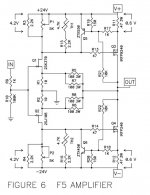
Thanks for your nice words, schematic is for the Pass F5… you can see attached. The layout is a work in progress, not finished and power traces will be thicker, left side (IRFP240) is finished but the right side is only a mirror for the moment, the idea was mainly to show the local decoupling with separate power ground for each cap and near the power tranies with actually three separate traces to the load.
R11 + R11B sum 0.47R and is the source load.
There is no ground plane, it's a one side PCB. Signal ground lands at the input with signal and from there we have a connection to star ground near the PSU. As far as you may see the circuit doesn’t allow many ground options. I have an F5 amp working with that exact arrangement with no trouble but if you see better ways to handle the ground I'm all ears.
Cheers, Tony
Attachments
Last edited:
Tom
Thanks for your nice words, schematic is for the Pass F5… you can see attached. The layout is a work in progress, not finished and power traces will be thicker, left side (IRFP240) is finished but the right side is only a mirror for the moment, the idea was mainly to show the local decoupling with separate power ground for each cap and near the power tranies with actually three separate traces to the load.
R11 + R11B sum 0.47R and is the source load.
There is no ground plane, it's a one side PCB. Signal ground lands at the input with signal and from there we have a connection to star ground near the PSU. As far as you may see the circuit doesn’t allow many ground options. I have an F5 amp working with that exact arrangement with no trouble but if you see better ways to handle the ground I'm all ears.
Cheers, Tony
Tony,
Totally-crazy idea: Use a two-sided PCB. <grin>
Seriously, I made two-sided PCBs by hand, all the time, a few years ago, and with MUCH-smaller features and larger board sizes, with just a 20-year-old laser printer, some paper, and a clothes iron (and some swimming pool acid and drugstore H2O2), "in under an hour" from computer to copper. Traces and trace-separations down to 0.01 inch were like child's play. I also put a component-layout "silk-screen" on every board, since it was so easy and quick to do. I "think" that I documented the 2-sided techniques that I developed (along with documenting the basic board-making process), at http://www.fullnet.com/gooteepc.htm . [And much better info than mine is probably now available in the Homebrew_PCBs discussion group, at yahoogroups.com.]
I actually quit using protoboards (especially those white ones with the plug-in rows of holes), beacause it was so quick and easy to make a pcb that would be so much more reliable (i.e. trustable) in its performance. I made at least one a day, for a while, back then.
It will help a lot if you have good PCB-specific software, since doing "copper pours" that automagically flow around (but don't touch) existing copper would make it much more practical.
Back when I started doing my first one-sided boards, I was using MS Paint! It worked. But wow was it tedious (although not as bad as people might imagine, once you get a "library" of your hand-drawn "component footprints" all saved in one big bitmap file).
Cheers,
Tom
Last edited:
If one really wants to worry about, and really understand where the parasitic characteristics of high performance decoupling caps -- ie, low ESL -- come into the equation this paper describing the difficulty of measuring, getting the numbers to, say, plug into a simulation tells a lot: How to Measure Low-ESL Tantalum Polymer, http://ecadigitallibrary.com/pdf/CARTSUSA09/5.1a reed.pdf
Frank
Frank
Last edited:
Capacitors don't usually have much inductance of their own, do they? Maybe 2 nH even for fairly big ones, in the actual capacitor element? I thought that the rest always turned out to be the inductance of the physical geometry, i.e. the leads and the conductive distance between the leads or the connection points (for SMDs).
So a 1 uF cap would be better for high frequencies than a smaller-value cap, IF it could be in the same size package. But we're not talking GHz here, anyway.
There are some good capacitor articles out there:
Capacitor Characteristics
Pro Audio Design Forum • View topic - Cyril Bateman Capacitor Sound Archive
capacitor self resonant frequency; Scandals in Electromagnetic Theory
Electromagnetic Theory; Maxwell's Equations; Ivor Catt
And just for (more) fun, "Why tubes and solid state sound different":
?House of Fire?: Firebottles And Groove Tubes Versus Devices That Find Their Origins in Sand (Part 1)
Tony,
Totally-crazy idea: Use a two-sided PCB. <grin>
Seriously, I made two-sided PCBs by hand, all the time, a few years ago, and with MUCH-smaller features and larger board sizes, with just a 20-year-old laser printer, some paper, and a clothes iron (and some swimming pool acid and drugstore H2O2), "in under an hour" from computer to copper. Traces and trace-separations down to 0.01 inch were like child's play. I also put a component-layout "silk-screen" on every board, since it was so easy and quick to do. I "think" that I documented the 2-sided techniques that I developed (along with documenting the basic board-making process), at http://www.fullnet.com/gooteepc.htm . [And much better info than mine is probably now available in the Homebrew_PCBs discussion group, at yahoogroups.com.]
I actually quit using protoboards (especially those white ones with the plug-in rows of holes), beacause it was so quick and easy to make a pcb that would be so much more reliable (i.e. trustable) in its performance. I made at least one a day, for a while, back then.
It will help a lot if you have good PCB-specific software, since doing "copper pours" that automagically flow around (but don't touch) existing copper would make it much more practical.
Back when I started doing my first one-sided boards, I was using MS Paint! It worked. But wow was it tedious (although not as bad as people might imagine, once you get a "library" of your hand-drawn "component footprints" all saved in one big bitmap file).
Cheers,
Tom
Sorry. The PCB-making link should have been http://www.fullnet.com/~tomg/gooteepc.htm .
(Please note that there is no longer ANYTHING for sale on ANY of my webpages.)
Last edited:
What counts is the total package -- you buy a cap and what you have to work with is where the leads emerge from the device. Which is why some of the ultra low ESL cap devices use a matrix of "pimples" under the belly to connect to the trace -- yer average DIY techniques not available here!Capacitors don't usually have much inductance of their own, do they? Maybe 2 nH even for fairly big ones, in the actual capacitor element? I thought that the rest always turned out to be the inductance of the physical geometry, i.e. the leads and the conductive distance between the leads or the connection points (for SMDs).
At high frequencies ESL is everything, absolutely everything; the nominal capacitance is virtually irrelevant. Yes, once you're over the 100MHz barrier, you have to work hard, really hard to gain every little bit of true decoupling, it becomes an artform to make it work.So a 1 uF cap would be better for high frequencies than a smaller-value cap, IF it could be in the same size package. But we're not talking GHz here, anyway.
To my mind, Jung's regulator is getting as close to as good as it gets in terms of supply impedance: possible to hit single micro ohms at low audio freq's, then starts to climb to about 0.1 milli ohms at 10kHz, 1 milli ohms at 100kHz, then you start to juggle very small multi-layer ceramics to try and keep things around 10's of milli ohms to as high a frequency as possible. But, finally lead length gets you, you can't escape it, and impedance will be around 1 ohm at 1GHz.
Frank
Last edited:
interesting thread. herewith my $0.02:
Rectifiers: these have both FORWARD and REVERSE recovery. Reverse recovery takes some doing, but forward recovery is easy to measure with a pulse generator and a scope. I suspect this has a lot to do with rectifier reliability decreasing as C increases - the bridge conduction angle decreases and the peak current increases, giving the diodes a much harder time. This is one reason why bigger =/= better (unless, of course, one designs the entire system as a whole).
then there is the trasformer secondary leakage inductance. pretty much no LF transformers have interleaved windings - P & S are usually separated, which is even worse (maximises leakage inductance). power systems engineers refer to this in PU terms - and a good transformer has 5-10% impedance. a bad transformer has 15-20%. A variac or gen set is much worse.
I ran into this a few years back doing startup tests on a 100W PFC smps. So I had a couple of 2kVA isolating transformers fabricated with interleaved windings (1/2P,S,1/2P) I also had several taps - 185Vrms, 230Vrms, 265Vrms so I can do high, nom & low line startup (also made a 230:110V version). I forget the exact numbers, but I got the secondary leakage down from mH to uH, and my startup tests started behaving like reality - the PFCs occasionally blew up on startup, but mine never did - until I lowered the supply impedance.
Lsec_leakage and Cdc form an LC resonant circuit that shapes the current during bridge conduction. this, too, needs to be taken into account during simulations, and further constrains usable cap range. Toroids of course inherently have better coupling than E-cores, but again interleaving can reduce this.
magnetic memory re. inrush - oh hell yes. I designed a mag-amp style dimmer a few years ago, and this caused me no end of grief - it took a week and about 100 FETs (and 3 PCBs) before I measured exactly what was going on and could deduce this. its a beautiful measurement though - caught my 1R FETs with > 100Vds while they were on. I re-designed the transformer so that the peak flux density was 800mT, so it could double at turn-on without saturating. Oh, and this is a non-volatile phenomenon, which made it all the harder to diagnose. thats one lesson i wont ever forget.....
I would simply measure the supply output impedance, while the amp is operating at a variety of loads. I love my network analysers
Hi Terry, thanks for the contribution. You seem to be a power transformer guy.
Kindly also provide your thoughts on rule of thumb calculations for our typical 100 watt amp regarding the transformer specifications, for instance what VA you would recommend, what output impedance as well as what governs the impedance.
What should one expect the magnetizing current to be. What regulation one need to look for.
What determines magnetic field causing induced hum in the amp, etc. I think all the knowledge and information in this thread regarding the amp power supply would be appreciated by anyone that reads it.
Hi Nico,
I should add: diode into 50R, drive from a pulse generator with a decent rise time to measure forward recovery
re. calcs: as shown in this thread, 1mF~2mF/A is a pretty good start, but it ultimately depends on the design objective (eg acceptable dV at amp transistors) and very strongly on the construction.
After I read this thread I went and wandered through the DIY pics. almost all of them seem designed to maximise wiring inductance. I'm a SMPS designer, and I started out designing AC motor controllers - the biggest we made was 1MW. when you have 6 x 1200V/300A IGBT hard paralleled you immediately discover stray inductance (edge-to-edge was about 450mm).
I use multilayer heavy-Cu PCBs for my designs, I always twist wires (plaiting works great for a center-tapped winding) and prefer to use planar transmission lines (our DC bus caps were bolted to a pair of 2mm Al (or Cu for the big ones) plates separated by 1mm lexan. its pretty easy to get stupidly low inductance like that.
I would carefully design my LF transformer for minimum leakage, have a low-inductance (direct) connection to rectifier & first bank of (many in parallel - low ESR, low ESL, lots of surface area for cooling) caps, a planar transmission line to the amp with a bit of series R, and another parallel cap bank at the amp.
induced hum, like all noise problems, comprises three parts:
1. a source
2. a coupling mechanism
3. a receiver
and the fix involves reducing/removing one or more these.
Source:
the H field has to come from somewhere. and that somewhere is generally either flux spewing out of a transformer (hence belly bands), or an inductor. and by inductor I mean current-carrying conductor. like a transformer wire, or a zobel coil or a W/W resistor lead or a PCB trace.....
For mains hum its pretty clear that the DC cap charging currents are the source. you can minimise these with judicious choice of cap value, and alas all efforts to stiffen up the supply at LF make these worse.
Coupling Path:
the path is the mutual coupling between the xfmr/rectifier/capacitor/amp wiring and the small- and large-signal stages. you arent in practice going to shield this (mumetal isnt cheap) so you have to minimise the mutual inductance at source and receiver to minimise the resultant field. twisted pair is your friend - if the twist length is small compared to the wavelength, there is a significant reduction H-field as adjacent loops are antiphase.
Receiver:
decent layout will fix this. single-sided = great way to maximise H-field susceptibility. but >= 2 layers doesnt necessarily help - I get a lot of work fixing lousy layouts, and I've seen many 6-layer PCBs that are appalling. Current Flows In Loops - Minimise Them. And dont chop bloody great holes in your 0V & power planes. seriously. I set up minimum via-via clearances so pours can flow inbetween them. this prevents me ever cutting slots (and "inverse" planes in cad packages really dont help here as they prevent you from seeing what the actual copper looks like)
beware sneaky inductors - crack the insulation off a PR02 resistor, or most WW resistors. I like the Panasonic ERJ-P series of SMT resistors, they have fantastic pulse handling ability and awesomely low ESL.
most of the audio amp layouts that I have seen have been single-sided and appallingly bad. actually, thats unfair - almost every PCB layout I've ever looked at has been bad. minimum PCB cost is not necessarily optimum wrt EMI.
On the ground
Here are a few threads why onboard caps may not really need to be big
http://www.diyaudio.com/forums/solid-state/198500-symef-amplifier-16.html#post2847427
http://www.diyaudio.com/forums/solid-state/198500-symef-amplifier-57.html#post3031930
Here are a few threads why onboard caps may not really need to be big
http://www.diyaudio.com/forums/solid-state/198500-symef-amplifier-16.html#post2847427
http://www.diyaudio.com/forums/solid-state/198500-symef-amplifier-57.html#post3031930
- Status
- This old topic is closed. If you want to reopen this topic, contact a moderator using the "Report Post" button.
- Home
- Amplifiers
- Power Supplies
- Power Supply Resevoir Size