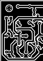
DC & clipp detection
Hi guys,
Here is the PCB of Quasi DC detect with added clipp detection. I hope someone will found it usefull. I found clipp detection circuit on Marshall Leach websait: http://users.ece.gatech.edu/~mleach/lowtim/graphics/clip.pdf .
Regards,
Miodrag Pejin
Hi guys,
Here is the PCB of Quasi DC detect with added clipp detection. I hope someone will found it usefull. I found clipp detection circuit on Marshall Leach websait: http://users.ece.gatech.edu/~mleach/lowtim/graphics/clip.pdf .
Regards,
Miodrag Pejin
Attachments
pejinm said:Also, if someone is interested I will post eagle files too...
Hi pejinm, I would like to see the Eagle .brd/.sch files if you cared to post or send me an email. Thank you for sharing and your hard work.
Stan
pejinm said:Also, if someone is interested I will post eagle files too...
Hi Pejinm,
I second your offer to post the Eagle files. I have tried yet again to enter the module schematic into the freeware Linux version of Eagle. Did you create the PCBs via the free version of Eagle? I am assuming it would have been the Windows version.
All others,
As an aside for those interested I have actually created 1, 2, 3, 4, and 5 pair versions of the module without DC protection, as well as revised versions of the 1,2, and 4 pair versions I created almost a year ago whose main update is the correction to the Vbe trace error Shawn found. I have not had time to post them to the web site I created for the alternate board varients I created a year ago.
I do not have the software used to create the PCBs. I make these varients with additional comments on board by using a graphics editing program. The program I use is GIMP. Suffice to say it does take some time to effect the changes. I am know using the PCB layout software process is very time consuming as well based on my attempts to find one that really works and well throught through. Sadly the man I tried fell short in many respects, and my use of Eagle is for special case situations such as existing Eagle projects. It has been easier and more productive to use GIMP with the base PCBs of quasi than using the software I have tried.
The reason for the modules with no additional circuits as part of the module board was to allow others space options or ability to use alternate protection circuits using the module without the DC protection circuit. When quasi first published the module PCBs it was in fact without the DC protection circuit as quasi expected others wanted the ability to use their own protection circuit. quasi also published some time later the DC protection circuit as a PCB with a pair of the DC protection circuits on the board.
I have a couple more new matter postings. I will post in next day or two. Life here is still a challenge so my time to is still rahter limited. It looks like it will continue for a few months at least so my time on thread will be limited.
Regards,
John L. Males
Willowdale, Ontario
Canada
21 November 2006 06:15
Requests
To Only One of your guys,
Any one of your guys that are using the same PCB software as quai uses I need the following parts in single PDF. I have some modifications still outstanding for the PCB I like to use. I use a graphics editing program to effect the changes, nto to mention I use Linux so Windows based programs are basicaly off limits to my use.
What I need are:
1) A horizontal TO-126 device.
2) A vertical AND horizontial mounted TO-220 device.
3) A vertically mounted 2 watt metal film AND carbon resistor. Research suggests typical diameters 4.7mm - 5.7mm. If you can provide both the about 4.7mm and about 5.7mm that would be great, if not then the about 5.7mm would be fine.
All of these should have their respective lead pads and should not be interconnected. If you have to interconnect these parts for the PCB software that is fine. I can deal with it.
Quasi,
Could you extend the table you created with number pairs of IRF450 vs power/impedance/rail voltage table with number of output devices to add what fusing to use and value of R6? I think it would be handy to add those to this very useful table.
Regards,
John L. Males
Willowdale, Ontario
Canada
21 November 2006 06:37
Error and Clarifications
Quasi,
While I had been working on an alternate version of your current schematic "nchan mos schematic only 06-05-06.pdf" I discovered quite by accident C3 to T1 has break in line just before connection dot to C3 collector. I actually did not notice this in the PDF until I converted the PDF to a PNG image. Even then I did not noticed for a few days of working on the PNG versions of the schematic. One has to zoom in qith Acrobat Reader to see the break. I am not sure if the break would show when printing the schematic. The problem can be seen at the 200% zoom level but is much easier to see at >= 300%.
I checked back to the prior versions of the schematic created and all of the prior versions, including the currents version, with the current software you use have the problem. I do not know if this is a software bug on the PCB software or not.
C7 is ideally considered a BiPolar. Most people use an electrolytic capacitor for a variety of reasons as I am sure you are aware. The PCB has a "+" symbol facing the signal gound. The questions are:
1) Is that "+" marking on the PCB if one is using a BiPolar capacitor?
2) If the "+" marking is when one uses an electrolytic capacitor instead is this the correct direction the "+" of the capacitor should face? I looked on the internet and diyAudio to find the answer. It seems from the research I have found a fairly even split based on the schematics. Some schematics show the "+" to face the feedback signal trace, others face the signal ground.
3) Any idea why there seems to difference of opinion what way the orientation of the "+" of an electrolytic capacitor from the feedback signal trace face or does this just boil down to personal preference?
While on the topic of the capacitor from the feedback signal line to the signal ground there seems to be some that order the resistor/capacitor to the signal gound order differently. In your BiPolar version of your amplifier you have the order reversed from the Mosfet version. The latter in a resistor/capacitor order and former is a capacitor/resistor order. Pros/cons, reasoning for choosing the different ordering of these two. The research I did on the internet/diyAudio shows both ordering choises being used in a fairly evenly divided manner.
As side unrealted question, I noticed your profile a few months ago that you had a flag of Greece and city name I cannot recall. Was that because you were out and about the "wide world"?
Life is still a major challenge here so I am not sure when I can have more time to be ask questions or contribute. I have some work in progress items when time permits related to this amplifier.
Regards,
John L. Males
Willowdale, Ontario
Canada
21 November 2006 07:15
Any Advantage to Filling Bottom of PCB?
Hi all,
I am just curious if there is any advantage to filling in the space on the botom of the PCB with copper. Some suggest there is added to inductance between traces while other sugest it reduces the inductance between traces. There is also mixed opinion to if the added inductance is if the fill area is or is not connected to a ground. I assume the ground that one would connect woudl be the signal gound, yes/no?
Thoughts, comments and/or prior references on this?
I have attached an example section of the quasi PCB to give you an idea of what I mean. Please be aware this was just a quickie fill. Some areas need to be removed manually as they are too small or isolated. Again this was done with a graphics editing program and not a PCB CAD program.
Regards,
John L. Males
Willowdale, Ontario
Canada
21 November 2006 07:26
Attachments
Hi,
The + is not personal preference, but to ensure the predominant voltage bias is in the correct direction to suit polarised electrolytics.
Some assemblers (not designers) of schematics do not realise that the input offset current puts a constant bias voltage onto the input terminal and similarly there is a matching bias voltage on the non-inverting input.
If the LTP input stage is made from PNP transistors the bias voltage is of opposite polarity to an LTP stage assembled with NPN transistors.
Some builder that did not appreciate the difference may assume that chance was coming into the equation.
However, the dual complementary LTP input stage has a partial cancellation of the input offset current and can with changes in environmental conditions have a bias that swaps polarity. Here it would be better to use a non-polar capacitor. But non-polar is better in most cases anyway. We only use eletrolytics to save space/money.
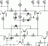
Pros/Cons to adapt in Leach Feedback Network
Hi all,
While looking for PCB images of TO-126, 2W resisitors, et al last week with no success I happened by accident to come across the:
diyAudio Forums > Top >Amplifiers >Solid State >Track layout design
http://www.diyaudio.com/forums/showthread.php?s=&threadid=86454
thread. Near end of the thread in Post #17
http://www.diyaudio.com/forums/showthread.php?postid=1008670#post1008670
was an explanation and supporting schematic "cf_vs_sf.pdf":
http://www.diyaudio.com/forums/attachment.php?postid=1008670&stamp=1158627260
explaining the pros of the feedback network in the Leach Amplifier. It appears this poster adapts this feedback network to the amplifiers he builds. I found the reading interesting.
I therefore looked the Leach Amplifier from the Leach Amplifier home site of W. Marshall Leach, Jr.:
http://users.ece.gatech.edu/~mleach/lowtim/
I was not sure how to determine parts values for the Leach amplifier feedback network and so far my questions on how these values are determined have gone unanswered. I know how the traditional feedback network determines the amplifier gain and the RC time constant in the traditional feedback network design used in many amplifiers and as quasi used.
I also looked at the excellent work of Jens Rasmussen again for help in what part values are used. Jens has a few Leach Amplifier threads and updates to modern parts which was one other design I had considered except for parts availability issues reduced my interest level:
http://www.delta-audio.com/Leach-Clone.htm
Between what very limited design knowledge I have of the feedback network, the Leach Amplifier site and Jens information I have tried to deduce the parts values that keeps the gain at 33 as quasi designed and maintains the feedback at and keeps R37 and R3 at same 33K0 value for least amount of DC offset wile keeping in mind the values quasi has spend so much time in deciding upon for his design.
I am not sure if C16 and C17 of the "cf_vs_sf.pdf" are really needed as the poster comments suggest mostly RF related. I have chose not to inlcue the C16 and C16 parts of "cf_vs_sf.pdf" in the Leach feedback varient of quasi's amplifier.
I am not sure my deduced values are reasonable or correct in adapting the Leach feedback network to quasi's amplifier. One of the qualities I like about the quasi amplifier is its simple and effective design. I am not sure if adding the extra few parts the Leach feedback network greatly degrades quasi's design or not assuming the Leach feedback network does not with the right parts values.
I would be interested in others far more in the know than I what their throughts in principle are to using the Leach feedback network are and of course more experienced experts on what changes in the feedback network parts values I have deduced may be required.
I have attached a schematic with the Leach feedback network adapted in with the best deduction for parts values I can make.
Again my time is very limited to a number of life challenges at moment. I needed a break form these so I have spent some of the time on this idea as well as update the PCBs I created almost a year ago. I do keep up reading and up to date with the thread. I generally just do not have the time to work on this project that much at moment I am sad to say.
Regards,
John L. Males
Willowdale, Ontario
Canada
21 November 2006 08:27
21 November 2006 09:36 The hoops and hops one has to go through to attach the original 25K 300 dpi graphic file 2475x1604 pixels, well below the 100K limit simply because it exceeds this imaginary 1000x1000 pixel additional limitation by diyAudio. I am techncially savvy, so I am able to maintian the image clarity/sharpness that most would not from software image rescale logic. I did not use the graphic rescale logic in usual sense. I cheated honestly") The first attempt created a file of 95K and very hard to read, but withing the 1000x1000 pixel limitation. Skip loading as file almost 4 times size and about 10 times as hard to read. The second attempt failed for same pixel limation reason due to strange diyAudio image math. Net of this effort is same rejected file created in a PDF document that covers a letter size page of 3300x2540 dpi and only 4K smaller simply because of some very advanced PDF related compression. I think someone at diyAudio needs to rethink this pixel limit restriction. Clearly the pixel restriction does not have as much impact as believed and for most of the less advance computer people causes what they may attach to be larger attachment than rejected file whilst the accepted file is much harder to read. My 2 cents worth opinion on matter anyway. jlm
The first attempt created a file of 95K and very hard to read, but withing the 1000x1000 pixel limitation. Skip loading as file almost 4 times size and about 10 times as hard to read. The second attempt failed for same pixel limation reason due to strange diyAudio image math. Net of this effort is same rejected file created in a PDF document that covers a letter size page of 3300x2540 dpi and only 4K smaller simply because of some very advanced PDF related compression. I think someone at diyAudio needs to rethink this pixel limit restriction. Clearly the pixel restriction does not have as much impact as believed and for most of the less advance computer people causes what they may attach to be larger attachment than rejected file whilst the accepted file is much harder to read. My 2 cents worth opinion on matter anyway. jlm
Hi all,
While looking for PCB images of TO-126, 2W resisitors, et al last week with no success I happened by accident to come across the:
diyAudio Forums > Top >Amplifiers >Solid State >Track layout design
http://www.diyaudio.com/forums/showthread.php?s=&threadid=86454
thread. Near end of the thread in Post #17
http://www.diyaudio.com/forums/showthread.php?postid=1008670#post1008670
was an explanation and supporting schematic "cf_vs_sf.pdf":
http://www.diyaudio.com/forums/attachment.php?postid=1008670&stamp=1158627260
explaining the pros of the feedback network in the Leach Amplifier. It appears this poster adapts this feedback network to the amplifiers he builds. I found the reading interesting.
I therefore looked the Leach Amplifier from the Leach Amplifier home site of W. Marshall Leach, Jr.:
http://users.ece.gatech.edu/~mleach/lowtim/
I was not sure how to determine parts values for the Leach amplifier feedback network and so far my questions on how these values are determined have gone unanswered. I know how the traditional feedback network determines the amplifier gain and the RC time constant in the traditional feedback network design used in many amplifiers and as quasi used.
I also looked at the excellent work of Jens Rasmussen again for help in what part values are used. Jens has a few Leach Amplifier threads and updates to modern parts which was one other design I had considered except for parts availability issues reduced my interest level:
http://www.delta-audio.com/Leach-Clone.htm
Between what very limited design knowledge I have of the feedback network, the Leach Amplifier site and Jens information I have tried to deduce the parts values that keeps the gain at 33 as quasi designed and maintains the feedback at and keeps R37 and R3 at same 33K0 value for least amount of DC offset wile keeping in mind the values quasi has spend so much time in deciding upon for his design.
I am not sure if C16 and C17 of the "cf_vs_sf.pdf" are really needed as the poster comments suggest mostly RF related. I have chose not to inlcue the C16 and C16 parts of "cf_vs_sf.pdf" in the Leach feedback varient of quasi's amplifier.
I am not sure my deduced values are reasonable or correct in adapting the Leach feedback network to quasi's amplifier. One of the qualities I like about the quasi amplifier is its simple and effective design. I am not sure if adding the extra few parts the Leach feedback network greatly degrades quasi's design or not assuming the Leach feedback network does not with the right parts values.
I would be interested in others far more in the know than I what their throughts in principle are to using the Leach feedback network are and of course more experienced experts on what changes in the feedback network parts values I have deduced may be required.
I have attached a schematic with the Leach feedback network adapted in with the best deduction for parts values I can make.
Again my time is very limited to a number of life challenges at moment. I needed a break form these so I have spent some of the time on this idea as well as update the PCBs I created almost a year ago. I do keep up reading and up to date with the thread. I generally just do not have the time to work on this project that much at moment I am sad to say.
Regards,
John L. Males
Willowdale, Ontario
Canada
21 November 2006 08:27
21 November 2006 09:36 The hoops and hops one has to go through to attach the original 25K 300 dpi graphic file 2475x1604 pixels, well below the 100K limit simply because it exceeds this imaginary 1000x1000 pixel additional limitation by diyAudio. I am techncially savvy, so I am able to maintian the image clarity/sharpness that most would not from software image rescale logic. I did not use the graphic rescale logic in usual sense. I cheated honestly
The first attempt created a file of 95K and very hard to read, but withing the 1000x1000 pixel limitation. Skip loading as file almost 4 times size and about 10 times as hard to read. The second attempt failed for same pixel limation reason due to strange diyAudio image math. Net of this effort is same rejected file created in a PDF document that covers a letter size page of 3300x2540 dpi and only 4K smaller simply because of some very advanced PDF related compression. I think someone at diyAudio needs to rethink this pixel limit restriction. Clearly the pixel restriction does not have as much impact as believed and for most of the less advance computer people causes what they may attach to be larger attachment than rejected file whilst the accepted file is much harder to read. My 2 cents worth opinion on matter anyway. jlmAttachments
Re: Post #1193
Hi Andrew,
Thanks for your reply. With the large gaps in my knowledge and guessing I never thought the LTP was a factor in the direction the "+" faces if one uses an electrolytic.
I know the ideal is to use a non-polar capacitor, but as we all know not practical nor afforable for a C7 like capacitor. I forgot where at moment, but in this thread there was mention for the actual voltage that C7 will likely see most of time it was noted the electrolytic at that voltage would behave like a BiPolar anyway. If the voltage raised higher than the typical operating levels it likely meant they would be much higher and therefore mean there is a problem with the amplifier in terms of assembly error or part defect.
I have seen designs where they parallel a film capacitor between 0.1 to 1uF with the C7 like feeback to ground capacitor. Would this paralleling approach help deal with the compromise of not using BiPolar? I can buy a MKP 1.5uF cap for about $0.50, or a 6.8 MKP for $3.00 to parallel C7 if that is better than just a 100uF electrolytic.
Some suggest using two electrolytics in series to make a BiPolar, but there are opinions suggesting that is not as good as a BiPolar. Of course some opinions seem to not favour the BiPolar as the BiPolar has its own shortfalls.
Everyone agrees using a non-polar capacitor is best, but also know for a C7 like capacitor it is not practical.
What if I just used a 6.8uF non-polar capacitor with a 14.7K resistance which would still keep the 100ms RC time constant for R18/C7? Would that have any downside? I am not sure where I may have read, if in fact I did, that it is important to keep the feedback resistors used for gain low to reduce noise in the feedback signal? True?
Regards,
John L. Males
Willowdale, Ontario
Canada
21 November 2006 10:09
Hi folks,
Just got back from Sydney. Quite a few questions here so I'll just cover the polarised feedback capacitor thing and the modified feedback circuit.
In theory a correctly adjusted amp should only have a few millivolts of offset at the output. This voltage will appear across the feedback capacitor but is so small that the polarity is practically irrelevant. If you can get a non-polar cap to fit by all means, but I have never had a problem with using a polarised cap.
I doubt the modified feedback circuit will make much difference given the component values used. At RF bands C15 will actually increase the gain of the amplifier and this is bad. The 10pF capacitor (C8) was intended to reduce the gain of the amp at RF frequencies and should be restored as it was.
Cheers
Q
Attachments
csv?
Hello,
Im new to the forums and new to audio electronics.
The Quasi amp looks a beast and this thread is a moster!
i have been reading through the posts for most of the afternoon... there is lots of great information here but it is pretty unwieldy!
Maybe it would be good to place the various designs and some of the relevant into a CVS type system so that all revisions can be easily navigated.
If you are interested i dont mind setting one up over at freashmeat or sourceforge.
Hi
concurrent version system. Its a database system normally used for computer source code, where by file revisions are stored in a "source tree". If someone wants to modify a branch of the project tree the file is checked out, modified, then the differences are committed back to the tree with a new version number.
With the amount of pages to get through and the number of "can you send me the latest version?" posts in this thread i thought placing the schematics and layouts relating to this amp in a CVS would be useful. The files could be separated from the disscussion and also all versions could be easily accessed.
www.sourceforge.net is a free repository for open source software development but there is some hardware stuff in there too. Im not sure but i dont see any reason why circuit designs cant go in there.
- Home
- Amplifiers
- Solid State
- Power amp under development