Yellow if I have to choose. The salesman (auction on the net) sold it as amber though.Samuel Jayaraj said:Radioman62, is it yellow or amber (orange) LED? I tried orange, it didn't work.
This morning I tried only two diodes in the string instead of three. The voltage drop is close to 1.5 volts. Bias setting is not so sensitive but the distortion sets in too early.
I think it is very sensitive either way. I use a 10 turn quality trimpot, but i have 500 ohm instead of 200. I think I also have to trim the resistor above to a higher value.
There is large differences regarding the trim settings, between resistor or diode(s) (R21).
Ohh, I wouldn't dare go that high from now on. My modules goes phoffIn any of the configurations, the minimum bias I am able to get is between 60 and 70mA. Ofcourse, distortion is worse compared to Iq of say 170mA.

I have zero bias all the way up to the last turns of the pot. But then again, it goes fast upwards

Maybe, but I can't see what it should be. I only have about +-39 volt on full effect 8ohm.It appears that supply voltage of less than +- 45 volts is just not suitable for the NMOS amp, unless some other component values are changed significantly.
Another thing is that, you and me Samuel, doesn't use the same devices or maybe not even the same module? I have the little one with one pair of IRFP260.
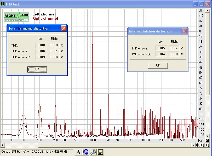
Some THD measurements on NMOS200
Take these figures with a pinch of salt. I haven't used this software that much before (Right Mark Audio Analyzer 5.3) and the rig wasn't perfectly setup. Soundcard is external M-Audio Audiophile USB set at 24bit 194kHz. Frequense responce limited to 20kHz.
I was about 5dB to low to really fill all the bits of the soundcard. Anyway, it was a fast setup to compare the looptroughcannel (Left channel) with the ampmodule NMOS200 (Right cannel) Ampmodule is just below clipping.
The listening sessions have to wait until I get more IRFP260 devices and also I wouldn't dare using these modules without DC protection on my speakers. I have to build such a unit first.
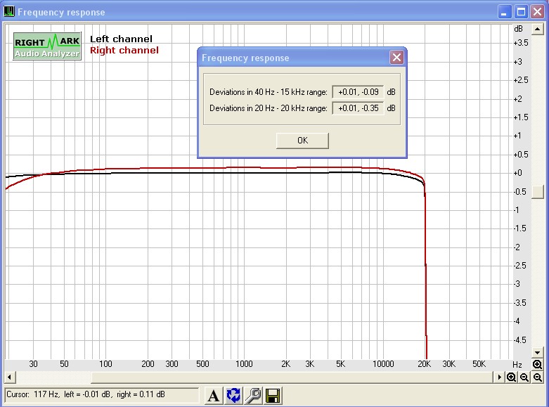
AndrewT said:Hi Radio,
can you identify any reasons for the left channel to consistently perform better than the right?
Yes, it's loopthrough the soundcard. Read the post again. Maybe an unususal way to test but the other module is not working and this was a way to compare the reference with the D.U.T. All is shown in one picture.
The reports in html from this software crash on me so I can't use them.
Hi,
congratulations, this looks fairly good, I'd say.")
A couple of questions:
- Can you eliminate the humming problem (that shows through at 50Hz and 200Hz)? It might explain a lot of the residual distortion (intermodulation). Powering the Audiophile USB via an external PSU usually helps a lot.
- Can you reduce to 24bit/48kHz? Many consumer audio equipment interfaces (such as most M-Audio products) suffer from raising THD+N at high sampling rates!
- Does your module's input filter explain the low frequency drop? It looks like the low pass at the input, with cuttoff around 15Hz with -6dB/oct., so that might be okay.
Thanks,
Sebastian.
congratulations, this looks fairly good, I'd say.
A couple of questions:
- Can you eliminate the humming problem (that shows through at 50Hz and 200Hz)? It might explain a lot of the residual distortion (intermodulation). Powering the Audiophile USB via an external PSU usually helps a lot.
- Can you reduce to 24bit/48kHz? Many consumer audio equipment interfaces (such as most M-Audio products) suffer from raising THD+N at high sampling rates!
- Does your module's input filter explain the low frequency drop? It looks like the low pass at the input, with cuttoff around 15Hz with -6dB/oct., so that might be okay.
Thanks,
Sebastian.
What's that in plain english?Radioman62 said:
Yes, it's loopthrough the soundcard. Read the post again. Maybe an unususal way to test but the other module is not working and this was a way to compare the reference with the D.U.T. All is shown in one picture.
The reports in html from this software crash on me so I can't use them.
That's the way such measurements are intended with this kind of software.
I think it's called "loopback". One channel of the audio interface is used as a reference (in terms of gain and frequency response), the other channel contains the D.U.T. in the loop between it's output and input.
This way, the properties of the audio interface can be ruled out of the equation.
The more advanced way would be configuring the software to automatically "substract" the reference from the D.U.T.
Cheers.
Thanks sek. I will see if I can do a better, more clear, presentation next time i present some figures in this community.The test still showed there is some qualitys in this amplifier design.sek said:That's the way such measurements are intended with this kind of software.
I think it's called "loopback".
The more advanced way would be configuring the software to automatically "substract" the reference from the D.U.T.
This software, RMAA5.3, doesn't seem to have any "subtraction" facilities inbuilt. Anyone using something different that doesn't cost anything or just a little?
Re: NMOS200 Scope pictures
Radioman62,
With respect to your "My NMOS200 with 100 ohm R21. An ugly assymetric clipping." and "My NMOS200 with R21 exchanged with Yellow LED (1.9V) Much better clipping. Near symetrical" results can you advise what the load was on the output, the input signal level and any part manufacturer or parts value you are using that are different than the parts/values indicated in the NMOS200 schematic? My current understanding is you are using IRFP260's for the output devices, +/-39V rails, the noted change in part/values for R21. What are you using for a value for R7 and R18? As I understand you are using a 10 turn pot for VR2. Are the values unchanged for the input Filter, NFB and NFB to ground parts? What PCB design are you using?
Regards,
John L. Males
Willowdale, Ontario
Canada
05 March 2008 (06:10 -) 07:12
Official Quasi Thread Researcher
05 March 2008 (07:18 -) 07:25 Corrected wrong link reference, additional question and additional link references. jlm
Radioman62 said:Another thing is that, you and me Samuel, doesn't use the same devices or maybe not even the same module? I have the little one with one pair of IRFP260.
You are right that I am using my own PCB design and IRFP460 outputs. I also have a buffer between the LTP and VAS stages. If you are referring to the NMOS200 schematic, then I am using 330ohms for R4 & R9 and for R7 I have used 6k8 and 3k6 alternatively. If I don't make these changes, the distortion level is too high.
sounds like it is no longer an Nmos200 implementation.Samuel Jayaraj said:I also have a buffer between the LTP and VAS stages. If you are referring to the NMOS200 schematic,
Re: Re: NMOS200 Scope pictures
 Hope you don't mind
Output load on ampmodule is allways 8 ohm in all tests I have done. Input signal I don't know. As designed by Quasi, a bit above 2 V p-p. As I said in my earlier post, just before clipping into 8 ohm. PSU voltages about +- 39 volt with that load.
I have used Quasis design, quasis PCB and component choices all trough, exept for the 500 ohm Bias trimpot instead of 200ohm, 47pF Millercap instead of 39pF and last, C12, C14 and C8 is 330uF instead of 100uF. I think none of these changes do something in the areas where I have put my cheek into this designs plus or minus
Cheers John, I compressed all your Qkeypunch said:Radioman62,
can you advise what the load was on the output, the input signal level and any part manufacturer or parts value you are using that are different .....
What are you using for a value for R7 and R18?
.... Are the values unchanged for the input Filter, NFB and NFB to ground parts? What PCB design are you using?
Regards,
John L. Males
Willowdale, Ontario
Canada
Hope you don't mind Output load on ampmodule is allways 8 ohm in all tests I have done. Input signal I don't know. As designed by Quasi, a bit above 2 V p-p. As I said in my earlier post, just before clipping into 8 ohm. PSU voltages about +- 39 volt with that load.
I have used Quasis design, quasis PCB and component choices all trough, exept for the 500 ohm Bias trimpot instead of 200ohm, 47pF Millercap instead of 39pF and last, C12, C14 and C8 is 330uF instead of 100uF. I think none of these changes do something in the areas where I have put my cheek into this designs plus or minus
I do power my Audio-m extrnal soundcard with the external PSU.sek said:Hi,
congratulations, this looks fairly good, I'd say.
A couple of questions:
- Can you eliminate the humming problem (that shows through at 50Hz and 200Hz)? It might explain a lot of the residual distortion (intermodulation). Powering the Audiophile USB via an external PSU usually helps a lot.
The setup with the loose "girlshair twining" ac cords and testcables all over, must degrade the 50,100 and 200 hz noicefloor, indeed.
Offcource. I will try that next time around. I weakly recall though that I got the lowest noicefloor with this setup.- Can you reduce to 24bit/48kHz? Many consumer audio equipment interfaces (such as most M-Audio products) suffer from raising THD+N at high sampling rates!
It's Quasis design. Maybe one could "up" the input capacitor. But the PCB layout doesn't have room for that.- Does your module's input filter explain the low frequency drop? It looks like the low pass at the input, with cuttoff around 15Hz with -6dB/oct., so that might be okay.
Samuel Jayaraj said:
You are right that I am using my own PCB design and IRFP460 outputs. I also have a buffer between the LTP and VAS stages. If you are referring to the NMOS200 schematic, then I am using 330ohms for R4 & R9 and for R7 I have used 6k8 and 3k6 alternatively. If I don't make these changes, the distortion level is too high.
Samuel, I think you are to much "off" to be compared and supported by Quasi.

On the other hand, the only "big" difference I see that would make the design "off" is that you have your own PCB design, and also the other output devices. Those two things can considerably change the design.... I think... maybe. I'm just doing the "rust off" instruction for myself. I'm going from a electronic maintenance guy with wide knowledge but narraow knowledge around the last 20 years of poweramplifiers this or that.
Drinkin' wine again and feelin' cheered up
 I can tell you all that Im in the 5'th chapter of Randy Sloanes book and about to start the real session of Douglas Selfes's masterpise aswell. They are similar in their statement about subjectivism. I love that, because I'm in the the same thoughts and have the same backround, allthough I respect som subjectivism when it comes to listening sessions. As soon as people don't mention which direction the speakercable goes..... Then I'm not following the subjectivism's corner
 I understand opinions that I am not following the original Quasi NMOS200, since I have designed the PCB myself and have changed certain values.
However, I had reported months ago that the original values resulted in audible distortion with 3 pairs of IRFP450s and +-63 volt supplies. I was able to solve the problem by changing the values of the upper CCS from 470E to 330E and reducing the lower Current Mirror feed resistor from 18K to 10K.
Just to be sure, I left R4 & R9 at 330E, changed R7 to 10K and R21 remained at 100E. The output was still a single pair of IRFP460s. The buffer before the Vas was retained. Then I plugged in rails of +-60 volts. With Iq of 120mA, the output is really clean to the ears. Lower Iq does not fully turn on the output devices. Changing the rails to +-45 volts dramatically lowered performance and even with Iq of 160mA, some distortion could be heard at high drive levels.
Further with the same boards, I brought back all R values to original Quasi NMOS200; with buffer in place and replacing R21 with a Yellow LED, I used rails of +-45 volts. Adjusting Iq to 130mA and even 150mA, at high drive levels distortion could be slightly heard.
Hence, for the benefit of other builders, my present tentative conclusions are:
1. OP devices with lower input capacitance is more suited for this amp.
2. Low supply rails do not particularly suit the amp.
3. Replacement of R21 with a Yellow LED gives an overall benefit. (Note that I did not find the bias adjustment to be sensitive as the case was with a string of 3 IN4148 diodes.)
4. At rail voltage of +-60 and above, R21 can remain as 100E.
Re: Re: Re: NMOS200 Scope pictures
I do not mind at all.
Pure resistive, the actual speakers you are using, a resistive/cap network to simulate a speaker load, etc?
The 330uF for C12/14 is fine, as that was the NMOS350 value. If anything a higher value improves an amp design, but at "diminishing" returns. I suspect for reasons of compactness C12/14 were indicated as 100uF for the NMOS200. C8 as 330uF is good and will just improve the RC time constant of the NFB to ground. I am not sure about the miller cap, but in the past quasi has indicated to builders challenged finding the value indicated their alternate choice based on local part availability to be ok.
Regards,
John L. Males
Willowdale, Ontario
Canada
06 March 2008 05:14
Official Quasi Thread Researcher
06 March 2008 05:28 Typo correction (after slow internet response!!!!).
Radioman62 said:
Cheers John, I compressed all your Q
I do not mind at all.
Output load on ampmodule is allways 8 ohm in all tests I have done.
Pure resistive, the actual speakers you are using, a resistive/cap network to simulate a speaker load, etc?
I have used Quasis design, quasis PCB and component choices all trough, exept for the 500 ohm Bias trimpot instead of 200ohm, 47pF Millercap instead of 39pF and last, C12, C14 and C8 is 330uF instead of 100uF. I think none of these changes do something in the areas where I have put my cheek into this designs plus or minus
The 330uF for C12/14 is fine, as that was the NMOS350 value. If anything a higher value improves an amp design, but at "diminishing" returns. I suspect for reasons of compactness C12/14 were indicated as 100uF for the NMOS200. C8 as 330uF is good and will just improve the RC time constant of the NFB to ground. I am not sure about the miller cap, but in the past quasi has indicated to builders challenged finding the value indicated their alternate choice based on local part availability to be ok.
Regards,
John L. Males
Willowdale, Ontario
Canada
06 March 2008 05:14
Official Quasi Thread Researcher
06 March 2008 05:28 Typo correction (after slow internet response!!!!).
Samuel Jayaraj said:I understand opinions that I am not following the original Quasi NMOS200, since I have designed the PCB myself and have changed certain values.
However, I had reported months ago that the original values resulted in audible distortion with 3 pairs of IRFP450s and +-63 volt supplies. I was able to solve the problem by changing the values of the upper CCS from 470E to 330E and reducing the lower Current Mirror feed resistor from 18K to 10K.
Just to be sure, I left R4 & R9 at 330E, changed R7 to 10K and R21 remained at 100E. The output was still a single pair of IRFP460s. The buffer before the Vas was retained. Then I plugged in rails of +-60 volts. With Iq of 120mA, the output is really clean to the ears. Lower Iq does not fully turn on the output devices. Changing the rails to +-45 volts dramatically lowered performance and even with Iq of 160mA, some distortion could be heard at high drive levels.
Further with the same boards, I brought back all R values to original Quasi NMOS200; with buffer in place and replacing R21 with a Yellow LED, I used rails of +-45 volts. Adjusting Iq to 130mA and even 150mA, at high drive levels distortion could be slightly heard.
Any chance you can share the Vas buffer modification you used with us Samuel?
Samuel you would then suggest with the NMOS350 Iq be 120ma per device for total of 360ma? For NMOS500 that would be 600MA or 0.6A?
Hence, for the benefit of other builders, my present tentative conclusions are:
1. OP devices with lower input capacitance is more suited for this amp.
Ciss I assume you are referring to here? I have read over time different opinions on Ciss, Crss and Coss. The general gist of the discussions would state the primary concern of a MOSFET output design to be either:
a) Ciss (sum) ability to drive the total capatiance
b) Crss being more important than Ciss
c) Crss or Coss being lower more important than Ciss
d) Different discussions, pros and cons, surrounding the impact of paralleling vs single MOSFET output devices with the exception that all agree paralleling divides the output current load amongst the output devices.
I am no expert in such matters and have read discussions and explaintions on all of the above that make sense to my limited knowledge.
This would also suggest why builders have not encountered what Samuel and Radioman62 have experienced.
This certainly drives me to figure out the best way to build one module where I can easily change everything. If I knew how to best approach the MJE's heatsinking on a breadboard I give it a go. The output devices I just run tail wires from the breadboard to heatsink. The hope would be breadboarding or any alternate similar approach would not introduce other problems the PCB deals with nor hide the problems builders, Samuel and Radionman62 included, have experienced.
2. Low supply rails do not particularly suit the amp.
I have done some calculations to "scale" resistive values based on rail voltage that I still think has some merit. Can the "experts" offer their wisdom to my simple logic?
3. Replacement of R21 with a Yellow LED gives an overall benefit. (Note that I did not find the bias adjustment to be sensitive as the case was with a string of 3 IN4148 diodes.)
Why would diodes vs LED VS resistor vs (perhaps) zener affect the sensitivity of the bias? I can see the bias made need to be readjusted when changing the type of R21 device, but why such a magnitude of difference in the sensitivity of the bias pot response?
4. At rail voltage of +-60 and above, R21 can remain as 100E.
Samuel are you suggesting if Radioman62 used 100r0 for R21 and used -/+60-65V rail he would not see the crossover distortion nor square wave ringing he sees with his +/-39V rails?
As a side note I wonder how the NMOS350 MKII would behave? Maybe it is time to test out the NMOS350 MKII as Samuel (use KSEs not MJEs for example) and Radioman62 (rails +/- 39V)?
Regards,
John L. Males
Willowdale, Ontario
Canada
06 March 2008 (06:40 -) 07:27
Official Quasi Thread Researcher
06 March 2008 07:31 site bug caused posting before finished Iq comments. jlm
06 March 2008 07:33 Typo corrections. jlm
06 March 2008 07:35 Typo corrections. jlm
06 March 2008 07:37 Typo corrections. jlm
The Vas buffer circuit was given to me by a commercial designer who is also a member of this forum. Since he may be using this in his commercial designs, I am afraid I may not be able to share.
There are ofcourse, several discussions on this forum regarding the capacitance presented by Mosfets to the preceding stage. It has also been shown that the effective capacitance presented varies with supply voltage. This may be the reason as to why the Quasi amps have some issues with lower voltage operation.
Whether it is called NMOS350 or 500, with 3 pairs of IRFP450s and +-63 volt supplies, I set Iq at 115mA which gave me the best subjective performance.
But with the single pair of OPs being IRFP460 and rails of +-39 to 45 volts, only Iq of 160mA seems to help, whether R21 is 100E or replaced with LED/Diode string. As to the over-sensitivity of the multi-turn bias trimpot with the Diode string, I have no clue.
Though I have not faced any thermal issues, I feel that the Vbe multiplier circuit should be tweeked. With the successful 3 pair boards, when I increased the 0.1uF cap across Emmiter and Collector of the Vbe multiplier, increasing bias was just not possible. Normally within reasonable limits, this should not be the case.
In Quasi's NMOS350 MKII note that the real changes are in the current flowing through the front end. The Vas is now cascaded. The cascade presents an easier load to the LTP. The changes I have been trying all along have to do with the same two stages. Just looking at the MKII schematic, I suspect that the amp will sound more detailed but may sound a bit bright and metallic. It is just my estimation. Someone building it can report on the subjective aspects.
So, you add a secret extra circuit and expect us to tell you why your different amplifier refuses to perform as an Nmos does.Samuel Jayaraj said:The Vas buffer circuit was given to me by a commercial designer who is also a member of this forum. Since he may be using this in his commercial designs, I am afraid I may not be able to share.

- Home
- Amplifiers
- Solid State
- Power amp under development