Hi,
the purpose of the decoupling caps on the PCB are to reduce the modulation being imposed on the power rails.
To achieve this a high frequency cap would be best. Choose from 680uF ceramic or 680uF polypropylene or at worst 680uF polyester. just joking. At affordable cost most would put in a large electrolytic // ceramic to try & achieve best reduction of spikes etc. I would specify a LESR type or // with a 1uF PP // 100nF ceramic located at each main current consumer.
Because these caps are there to absorb high frequency missmash ( I had another word h.a.s.h. in here but the forum automatically edited it out) on the rails they are coupling the same contaminated spiky non signal (it did it again, c.r.a.p.) to their grounds. Do not connect these contaminated grounds to the signal ground. Instead wait until you get back to the main amplifier central star ground.
AndrewT said:
To achieve this a high frequency cap would be best. Choose from 680uF ceramic or 680uF polypropylene or at worst 680uF polyester. just joking. At affordable cost most would put in a large electrolytic // ceramic to try & achieve best reduction of spikes etc. I would specify a LESR type or // with a 1uF PP // 100nF ceramic located at each main current consumer.
Do not connect these contaminated grounds to the signal ground. Instead wait until you get back to the main amplifier central star ground.
Hi Andrew,
Thanks for you reply.
I need to clarify as I do not have enough knowledge to be certain about the high frequency cap comment/joke. Can one choose to use a 680uF ceramic or polypropylene rather than the electrolytic//ceramic/PP combination? Is it a case of cost or just nothing that large available in ceramic/PP? I hope that was not too silly a question.
With respect to the grounding comment you made, can I safely assume that based on the schematic of quasi's design this is accounted for? Some time ago I asked quasi about his grounding symbols used in the early schematic where ground was the noise ground and one was the quiet ground. I am assuming the current schematic, that uses different grounding symbols compared to early schematics, two grounds are one for signal/quiet and one for noisy ground, as was care in early schematics. I am assuming the symbol with a line and / / / below is the chassis AKA noisy ground, and the upside down T is the quiet ground for the current schematic. Assuming I am correct, is the current schematic is correct with respect to your comment of keeping the contaminated grounds from the signal grounds?
An interesting note is R2, which is 10R0, connects from the quiet ground (I am assuming) to the noisy ground AKA chassis ground. I am not sure if R2 is faciliting keeping the noisy ground from signal ground or not. I am not sure even what wattage rating R2 has in the event R2 is less about isolating noisy and quiet grounds and more about ground shock protection.
Regards,
John L. Males
Willowdale, Ontario
Canada
09 December 2005 14:49
Capacitors, grounding and layout
Hi John
In the schematic I tried to indicate the different grounds by using different symbols. This is to make sure that builders of this amp avoid tying components in the audio path to a "noisy" ground.
The 10-ohm resistor serves to decouple the two grounds. It can as you say also provide some protection should the main ground lose reference, in this case the 10 ohm resistor fries. I use a 1/2 watt metal film.
With respect to the output stage supply capacitors AndrewT has correctly advised that they filter out unwanted mash (didn't even try has...) that is picked by the supply leads from the main supply. The capacitors also provide a small amount of reserve to compensate for variations of the fuse resistance. These capacitors should be bypassed by polyester (or similar) 100nF as noted by AndrewT.
Also you will notice that the direction of the tracks feeding these is opposite to the track feeding the output stage from the fuse pad. This is critical. These capacitors draw large AC currents and even a short copper track can induce a voltage drop. If the capacitors were on the other side of the fuse pad then this voltage drop will appear as noise (hum & mash). By using the layout I have, the only current flowing through the output stage track is that required by the amp itself.
You may have noticed that the sizes of the capacitors on the board layout appear larger than those in the photos of my amp. This again as Andrew pointed out is because of the need for low ESR. I have boxes of broken computer power supplies each containing 2 x 200v capacitors. So I decided to alter the layout to take these low ESR (and free) caps.
Finally the input stage capacitor sets the low frequency roll-off of the amp. This is a personal choice.
Cheers
anatech said:Hi Quasi,
Is your friend's soft start in the preamp? Try a lower voltage relay and a resistor to compensate if that's the case.
-Chris
In my friends set-up the soft start is in the power amp. I take your point about using a lower voltage relay, it could however get too hot when the secondary voltage fully rises .....aaaah but maybe a zener could....sounds ok...I'll try it.
Cheers
Hi Quasi,
No, calculate the resistor in series with the coil to drop the excess voltage, a little more than you need so the relay has slightly lower voltage across the coil than spec. The pull in voltage is lower than the rated voltage. The hold voltage is lower still.
-Chris
No, calculate the resistor in series with the coil to drop the excess voltage, a little more than you need so the relay has slightly lower voltage across the coil than spec. The pull in voltage is lower than the rated voltage. The hold voltage is lower still.
-Chris
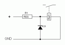
Yes but then we are back to maybe not getting enough voltage to pull it in under loud music conditions when turned on. I should use a series resitor as you say but also a 5 watt zener so that I can rely on a lower pull in voltage and then excess voltage is shunted away.
Attachments
Hi Quasi,
Sorry, I don't understand something. The amplifier is getting a high signal as it is turned on?
Your supply will not droop that much or it will burn out the surge resistor. Standard practice is to mute the input signal and disconnect the speaker load until the amplifier settles down. At this point the surge relay has already closed. The drop out voltage is much lower, so don't worry about that too much.
-Chris
Edit: omit D1 in your diagram and you have what I was suggesting.
PCB Size
Quasi,
Can you advise me what the dimensions of your amplifier PCB with the DC Detection circuit on the PCB is? I am trying to validate some odd behavior with differences different software casues in creating a PDF of the variant PCB files I created.
BTW, if anyone has a suggestion how I can make the PCB variants I created available I am all ears. Sadly, only a few of PCB image varients result in less than the 100K diyAudio attachment limit ... no matter if I reduce the DPI to 300 and/or create a PDF from a single image. All of the top/component layouts are all well over the 100K limit. This appears to be a comsequence of having to convert the original board PDFs to a graphic file format. I suspect the original board PDFs were stored in some sort of vector based manner which takes up less space in a PDF.
Regards,
John L. Males
Willowdale, Ontario
Canada
10 December 2005 13:24/13:26
Quasi,
Can you advise me what the dimensions of your amplifier PCB with the DC Detection circuit on the PCB is? I am trying to validate some odd behavior with differences different software casues in creating a PDF of the variant PCB files I created.
BTW, if anyone has a suggestion how I can make the PCB variants I created available I am all ears. Sadly, only a few of PCB image varients result in less than the 100K diyAudio attachment limit
... no matter if I reduce the DPI to 300 and/or create a PDF from a single image. All of the top/component layouts are all well over the 100K limit. This appears to be a comsequence of having to convert the original board PDFs to a graphic file format. I suspect the original board PDFs were stored in some sort of vector based manner which takes up less space in a PDF.Regards,
John L. Males
Willowdale, Ontario
Canada
10 December 2005 13:24/13:26
Re: Board Size and V1.4 Board Varients
Hi quasi,
Thanks for your reply.
Excellent, the images I created have still perserved actual size. I sorted out the PDF generation problem, typical unclear documentation about meaning of options.
Update 20051211 08:08
***************************
Ok, after some failed attempts with some free hosting sites that really have bad online Web Editors or various usability issues with their site editors and page space management tools I happened across a site
http://keypunch.white.prohosting.com/
that I was able to use to create some basic pages that have the edited varients of Quasi's board design re Post 238:
http://www.diyaudio.com/forums/showthread.php?postid=785310#post785310
and Post 239:
http://www.diyaudio.com/forums/showthread.php?postid=785318#post785318
I have managed with the online tools to create a set of pages that have the images of the board variants and some handy links to the basic current materials quasi has posted about his design.
When I have some time in week or two I will make some updates including PDF versions of the board variants I made from quasi's amplifier board design.
Quasi,
When you have time could you visually check the board variants I created to be sure they are correct? Also can you confirm that the unmarked retangular like componment outline beside T8 on the layout board image of your original file is a left over from a prior version of your circuit when that was used as a miller capacitor (it was removed in your final built design, likely after a few comments made that is was not necessary as was case with at least one other miller capacitor that was removed in your final built design).
BTW, not having looked for while at the original PCB amplifier boards, I know know why your reference to colour was made. The layout image of your board had the tracks as purple and the under the board wires a dark read. For the PDF it makes little difference to the PDF in terms of file size as the image is stored as vectors and layers.
History/Reference - 20051210 19:35 - 19:37
********************
The trace images are actually a black and white image as the original PDF for V1.4 with DC Detect. This means these images use the least amount of file space. I could create 300DPI based images and that would likley bring these down below the 100K file size limit. The problem lies with the silkscreen/shadow of traces (layout) images. These were imported as grey scale as the PDF of the layout image was a grey scale image. Even when I reduce the images to 300DPI the file size only reduces about 40% or so. This means these files were still in the 130k - 160K size depending on the number of output devices on the board.
I tried making .GIF and PDF images of each image, but this did not give me smaller file sizes, in fact the files were a bit larger than the .PNG file format I have them in currently and created in initially. I tried to convert the component/shadow trace images to what is called an indexed image seeing as there are only three grey scale colours - Black, not quite black and grey for components, under board insulated wires and shadow tracing. I was not able to convert to an index file for reasons I do not quite understand. Converting to index caused some odd problems where black and near black partly converted to the grey colour of the shadow traces.
I could convert to .JPEG, but my I suspect the the component/shadow traces may loose abliity to read the values and/or see the component traces. .JPEG is what we call a lossy type file. JPEG is like MP3 file lossy concepts, and .PNG is like a gzip compressed wave file. gzip is along lines of zip, meaning zip files do not loose data otherwise one could not get their data back from a zip file. I know JPEG is generally what digital cameras output, but in fact JPEG is a rather inferior image format. Sadly most of the mass consumer public is not aware of this fact. Hence companies continue to produce products using JPEG image formats.
I feel there is no point posting .JPEG images only to have people want a proper file like a PDF, .GIF or .PNG that will perserve all the bitmap data. A .JPEG will likely loose 30-50% of the image data to get below 100K for the component/trace shadow images.
I try to contact the diyAudio moderator to see what they suggest.
20051211 08:23 Update
Ok for now maybe we will not need the diyAudio moderator's assistance. Lets see how this works first with the free hosting web page:
http://keypunch.white.prohosting.com/
Regards,
John L. Males
Willowdale, Ontario
Canada
10 December 2005 19:35 - 19:57
10 December 2005 20:15 - 22:30
11 December 2005 04:00 - 08:39/08:44/08:45/08:46
Hi quasi,
Thanks for your reply.
Excellent, the images I created have still perserved actual size. I sorted out the PDF generation problem, typical unclear documentation about meaning of options.
Update 20051211 08:08
***************************
Ok, after some failed attempts with some free hosting sites that really have bad online Web Editors or various usability issues with their site editors and page space management tools I happened across a site
http://keypunch.white.prohosting.com/
that I was able to use to create some basic pages that have the edited varients of Quasi's board design re Post 238:
http://www.diyaudio.com/forums/showthread.php?postid=785310#post785310
and Post 239:
http://www.diyaudio.com/forums/showthread.php?postid=785318#post785318
I have managed with the online tools to create a set of pages that have the images of the board variants and some handy links to the basic current materials quasi has posted about his design.
When I have some time in week or two I will make some updates including PDF versions of the board variants I made from quasi's amplifier board design.
Quasi,
When you have time
could you visually check the board variants I created to be sure they are correct? Also can you confirm that the unmarked retangular like componment outline beside T8 on the layout board image of your original file is a left over from a prior version of your circuit when that was used as a miller capacitor (it was removed in your final built design, likely after a few comments made that is was not necessary as was case with at least one other miller capacitor that was removed in your final built design).BTW, not having looked for while at the original PCB amplifier boards, I know know why your reference to colour was made. The layout image of your board had the tracks as purple and the under the board wires a dark read. For the PDF it makes little difference to the PDF in terms of file size as the image is stored as vectors and layers.
History/Reference - 20051210 19:35 - 19:37
********************
The trace images are actually a black and white image as the original PDF for V1.4 with DC Detect. This means these images use the least amount of file space. I could create 300DPI based images and that would likley bring these down below the 100K file size limit. The problem lies with the silkscreen/shadow of traces (layout) images. These were imported as grey scale as the PDF of the layout image was a grey scale image. Even when I reduce the images to 300DPI the file size only reduces about 40% or so. This means these files were still in the 130k - 160K size depending on the number of output devices on the board.
I tried making .GIF and PDF images of each image, but this did not give me smaller file sizes, in fact the files were a bit larger than the .PNG file format I have them in currently and created in initially. I tried to convert the component/shadow trace images to what is called an indexed image seeing as there are only three grey scale colours - Black, not quite black and grey for components, under board insulated wires and shadow tracing. I was not able to convert to an index file for reasons I do not quite understand. Converting to index caused some odd problems where black and near black partly converted to the grey colour of the shadow traces.
I could convert to .JPEG, but my I suspect the the component/shadow traces may loose abliity to read the values and/or see the component traces. .JPEG is what we call a lossy type file. JPEG is like MP3 file lossy concepts, and .PNG is like a gzip compressed wave file. gzip is along lines of zip, meaning zip files do not loose data otherwise one could not get their data back from a zip file. I know JPEG is generally what digital cameras output, but in fact JPEG is a rather inferior image format. Sadly most of the mass consumer public is not aware of this fact. Hence companies continue to produce products using JPEG image formats.
I feel there is no point posting .JPEG images only to have people want a proper file like a PDF, .GIF or .PNG that will perserve all the bitmap data. A .JPEG will likely loose 30-50% of the image data to get below 100K for the component/trace shadow images.
I try to contact the diyAudio moderator to see what they suggest.
20051211 08:23 Update
Ok for now maybe we will not need the diyAudio moderator's assistance. Lets see how this works first with the free hosting web page:
http://keypunch.white.prohosting.com/
Regards,
John L. Males
Willowdale, Ontario
Canada
10 December 2005 19:35 - 19:57
10 December 2005 20:15 - 22:30
11 December 2005 04:00 - 08:39/08:44/08:45/08:46
Toroids VA Capability
Hi All,
Quasi's final design used a 500 VA 53-0-53V secondary Toroid. I have a couple of 44-0-44V toroids 960 VA (one is rated 1120VA). In the context of quasi's reply, Post 159:
http://www.diyaudio.com/forums/showthread.php?postid=600848#post600848
I am assuming I am safe to be able to run at least 3 amplifier modules from my 44-0-44V 960VA toroid. Could I run 4 amplifiers from this 44-0-44V 960 VA toroid? Each amplifier will have own rectifiers/filtering circuit, so there should be no need to discuss the power demands on the PSU circuits, correct?
With the example calcualtions of Post 159 would it be correct to assume the filter and other components of the PSU circuit voltage rating needs to be > 57.7 VDC? Of course I will give some safety/life margin considerations. The P-P of the PSU out is about 57.7 VDC per rail, while the output devices are seeing about a 50.7 VDC P-P?
Regards,
John L. Males
Willowdale, Ontario
Canada
11 December 2005 09:15
Re: PICTURE
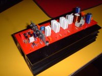
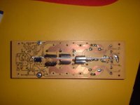
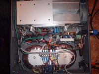
Well done zeonrider!! Looks better than professional.
Is that a PCB or some material that looks like PCB? I have never seen a fire red PCB.
Where did you find that wonderful heatsink? The 4 (at least) coloured bypass caps are what type? What guage of enamled wire for the output coil did you use?
Regards,
John L. Males
Willowdale, Ontario
Canada
11 December 2005 10:43
zeonrider said:Of course in FERRARI RED
Well done zeonrider!! Looks better than professional.
Is that a PCB or some material that looks like PCB? I have never seen a fire red PCB.
Where did you find that wonderful heatsink? The 4 (at least) coloured bypass caps are what type? What guage of enamled wire for the output coil did you use?
Regards,
John L. Males
Willowdale, Ontario
Canada
11 December 2005 10:43
Re: PICTURE
Resistors wrong, color inflicting sound (or brain)? Drivers cooled insufficiently
zeonrider said:Of course in FERRARI RED
Resistors wrong, color inflicting sound (or brain)? Drivers cooled insufficiently
- Home
- Amplifiers
- Solid State
- Power amp under development