Hello to all experts
Attached is a schematic I have "backengineerd from a power amp kit, which was assembled by a friend. He bought the kit around 1990 and fired it never up.
He gave me two single channel PCB's, already assebled, but without heat sink and power supply. And without any papers which would had helped me
Rail voltage - no info's, my guess is around ±40 to 50 Volts, according to the data sheets I found, it should be possible with 50 Volts and still good safety margin. Am I right?
Q3, R8, D1 - is this a current mirror? (Sorry, but my elelctronics knowledge is quite limited )
)
What do you think about the topology? Could it sound good?
I'm not shure wheter I should spend money on the power supply and give it a go.
Thanks to you all!
Tino
Attached is a schematic I have "backengineerd from a power amp kit, which was assembled by a friend. He bought the kit around 1990 and fired it never up.
He gave me two single channel PCB's, already assebled, but without heat sink and power supply. And without any papers which would had helped me
Rail voltage - no info's, my guess is around ±40 to 50 Volts, according to the data sheets I found, it should be possible with 50 Volts and still good safety margin. Am I right?
Q3, R8, D1 - is this a current mirror? (Sorry, but my elelctronics knowledge is quite limited
)What do you think about the topology? Could it sound good?
I'm not shure wheter I should spend money on the power supply and give it a go.
Thanks to you all!
Tino
Attachments
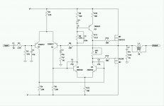
It looks like the Maplin MOSFET kit. I've built some, and they sound good to me. 100W RMS into 8Ohms with +/- 50v supply, or 150W into 4Ohms.
The design is based on the Hitachi application note for their MOSFETs. Many amplifiers were based on the app note design.
You are correct about the current mirror, I don't know how it compares with one using two transistors, but it works well enough.
I changed the value of R9 so that the collector voltages of TR3 and TR4 are the same. The bias of the whole design varies with the power supply voltage, but it's quiet (low noise) and doesn't thump at switch - on. I like its simplicity.
I have the documentation if you are interested.
Tino,
For such a simple design (not a bad thing) they sound very good. I still remember the first time I heard it (Maplins kit) – I’ve associated the sound with “MOSFET” designs ever since – IMHO you will find it hard to beat with a “commercial” amp anywhere near the price level.
I would recommend using say 20000uF (4 x 4700uF works very well) per rail for the PSU – PSU rejection is not that great.
Good luck, sit back and enjoy")
John
For such a simple design (not a bad thing) they sound very good. I still remember the first time I heard it (Maplins kit) – I’ve associated the sound with “MOSFET” designs ever since – IMHO you will find it hard to beat with a “commercial” amp anywhere near the price level.
I would recommend using say 20000uF (4 x 4700uF works very well) per rail for the PSU – PSU rejection is not that great.
Good luck, sit back and enjoy
John
Does this design require a regulated power supply? It probably would work better with one. I bet the PS regection would be better if the differential amp stages had a current source bias...or maybe a current source/mirror. Not suggesting you change anything but if quality is what your after...
Re; regulated power supplies
One mod I intend doing is to regulate the input and drive stages, but leave the output stage unregulated. I have a suitable transformer, but I need to make new PCBs to implement it. This will stabilise bias conditions.
I replaced R3 (input tail resistor) with a 1mA current source, but I get small thumps because the bias now needs a certain voltage to operate.
I would check on the value of R9 though, (from the original documentation as you will see shortly) as I mentioned previously. The documentation from Maplin is incorrect in their description of the differential VAS load; they call it a current source rather than a mirror. Depending on supply voltage, if the voltage across R9 is too high, it cannot pass sufficient current on positive half cycles. Too low and dissipation in the VAS transistor increases, and is imbalanced wrt the other.
I thought about other mods, but it just ruins the beautiful simplicity of the circuit.
Re: Re; regulated power supplies
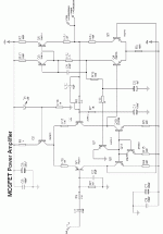
Nothing wrong with not being as simple as you initially want. If you use a regulated power supply, then forget the current source in place of the emitters' resistor in the diff amp. Use the emitters' resistor and include a currnet source and mirror circuit like I have drawn. This will give you much higer gain and power supply rejection, even if the output transistors are not regulated. As a matter of fact, you could probably eliminate the second diff amp stage and replace it with a single VAS transistor (biased with a current source of course). About the same number of transistors, just aranged differently.
johnnyx said:One mod I intend doing is to regulate the input and drive stages, but leave the output stage unregulated. I have a suitable transformer, but I need to make new PCBs to implement it. This will stabilise bias conditions.
I replaced R3 (input tail resistor) with a 1mA current source, but I get small thumps because the bias now needs a certain voltage to operate.
I would check on the value of R9 though, (from the original documentation as you will see shortly) as I mentioned previously. The documentation from Maplin is incorrect in their description of the differential VAS load; they call it a current source rather than a mirror. Depending on supply voltage, if the voltage across R9 is too high, it cannot pass sufficient current on positive half cycles. Too low and dissipation in the VAS transistor increases, and is imbalanced wrt the other.
I thought about other mods, but it just ruins the beautiful simplicity of the circuit.
Nothing wrong with not being as simple as you initially want. If you use a regulated power supply, then forget the current source in place of the emitters' resistor in the diff amp. Use the emitters' resistor and include a currnet source and mirror circuit like I have drawn. This will give you much higer gain and power supply rejection, even if the output transistors are not regulated. As a matter of fact, you could probably eliminate the second diff amp stage and replace it with a single VAS transistor (biased with a current source of course). About the same number of transistors, just aranged differently.
Attachments
One worthwhile and simple modification is to add say 33R resistors in series with each of the Emitters of the input transistor pair T1 & T2 (so that’s 2 resistors).
Adding input stage degeneration to an existing design should be done with care as the change OL gain could upset the amplifiers stability criteria. Slew rate will be reduced, but can be restored by increasing input stage current (reducing the value of R3) – something to play with – but watch the amplifiers stability!
This will reduce the OL gain slightly, but will reduce overall distortion and improve the input stage tolerance to RF (from say from an RF polluted input from a CD / DVD player). Typically making the amp sound smoother and less hard.
John
Hi cunningham,
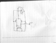
The input stage cann't have a current mirror load, because of the differential VAS. To turn it into a single ended VAS would be a re - design rather than a mod.
One idea I had, to retain the basic topology but improve bias stability, is shown in the attached diagram. This sort of arrangement I first saw in a valve (tube) amp. I forget the designer's name. But it spoils the simplicity.
Hi JohnW,
Yes, emitter degeneration is something to include in the new board layout. If the current is increased to give the same gain as before the resistors were added, then the stability margins won't change. Doug Self's book is good on things like that.
Attachments
Thanks to you all, you gave me confidence enough to look for the power supply and a heatsink. I'll mull about separate power supply for the driver stage and the MOSFET's, altough this means that i have to break up some traces on the board (or do a new one).
I did some search on the web, but didn't find any better information than those from you guys .
.
Cheers, Tino
I did some search on the web, but didn't find any better information than those from you guys
.Cheers, Tino
zinsula;
I've scanned the documents, but you've turned off your e-mail link in your profile. I'll send them when you get in touch. My e-mail link should work, if you want to do it that way.
thanh;
If you are referring to the one I posted, then it is my own experiment, hence the simulator probes attached to the image. There are no output transistors attached because I was experimenting with the voltage amplifier part. The idea is that feedback through the current mirrors sets the voltage at Q4 collector, and the bias current for the VAS stage is set by one resistor, R12.

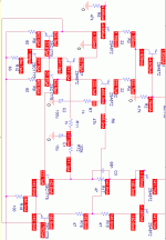
I wonder if the amp is a bit slow. I am not an expert about MOS. Please correct me if my reasoning below is wrong.
The MOS has input cap about 250pf. And the driving stage current is arout 3ma. Accoring to the formula
i*delta = c * delta v
we have 3ma * 1us= 250 p * delta v
Thus we get the roughle estimated slew rate about 12 V/us.
This is a bit slow if it is a high power amplifiier.
The MOS has input cap about 250pf. And the driving stage current is arout 3ma. Accoring to the formula
i*delta = c * delta v
we have 3ma * 1us= 250 p * delta v
Thus we get the roughle estimated slew rate about 12 V/us.
This is a bit slow if it is a high power amplifiier.
JohnW said:
Adding input stage degeneration to an existing design should be done with care as the change OL gain could upset the amplifiers stability criteria. Slew rate will be reduced, but can be restored by increasing input stage current (reducing the value of R3) � something to play with � but watch the amplifiers stability!
The VAS stage contributes the first pole. And normally the power transistor stage contributes the second pole. The pole of the differential stage is much far beyond. Thus I would think it safe adding degeneration resistor to the input differential pair.
robert_chien said:I wonder if the amp is a bit slow. I am not an expert about MOS. Please correct me if my reasoning below is wrong.
The MOS has input cap about 250pf. And the driving stage current is arout 3ma. Accoring to the formula
thanh said:this is the sim of that schematic
The resistor values came out fuzzy due to the compression needed to post it. It was ok as I intended only to show the ideas I had. 140mA in the VAS transistors is definitely incorrect, they would burn up very quickly. I think it should be 10mA in the original design, but I may have increased it for the mod.
If you are interested and send me an e-mail, I could send you the original. I use Proteus, but I can convert it to a Windows metafile with no loss of detail, it's 109k but too big to post.
- Status
- This old topic is closed. If you want to reopen this topic, contact a moderator using the "Report Post" button.
- Home
- Amplifiers
- Solid State
- Power Amp Schematic