I too agree with Fotios and AndrewT. But these past few years there was so much pressure from commercials by credit companies, to get that loan for the new car or the dream hollidays or the new LED TV or what ever - that people were made believe that this way of living was fine. On TV, newspapers, outdoors, website banners - you just couldn't miss the credit advertising! Add that to an economy that doesn't grow for the past 10 years and you get an explosive mixture. We have now to DIY our way out of this. And I believe we will!
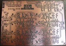
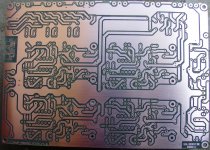
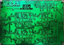
Lets get some fun, it is Easter time. When you don't have money left over, you make PCBs at home  . Here is the main PCB of preamplifier, presented in 3 pictures showing the process: In the first two you can see the PCB from both sides, drilled and cleaned before the tinning of power tracks and the soldering of the 27 via holes. After this, the PCB is cleaned again and is ready for varnishing. The final result is presented at the 3rd picture.
Have fun and Happy Easter!
. Here is the main PCB of preamplifier, presented in 3 pictures showing the process: In the first two you can see the PCB from both sides, drilled and cleaned before the tinning of power tracks and the soldering of the 27 via holes. After this, the PCB is cleaned again and is ready for varnishing. The final result is presented at the 3rd picture.Have fun and Happy Easter
!Attachments
Hi,
What is the green finish on the 3rd pic?
Is it solder resistant?
Why are a few traces a different shade of green?
There are solder pads on both sides. Do you intend soldering each through hole lead to both sides to mimic a PTH?
Hi Andrew
The green finish, it is not solder resistant. It is obtained with the use of a polyurethane based insulating - encapsulating transparent green varnish in spray can. It melts very easy with the tip of a soldering iron.
Traces that presents a different shade of green, simply are tinned before the varnishing.
Yes, i use spare lead wires from soldered parts for the via holes.
Hi,
What is the green finish on the 3rd pic?
Is it solder resistant?
Why are a few traces a different shade of green?
There are solder pads on both sides. Do you intend soldering each through hole lead to both sides to mimic a PTH?
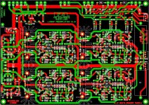
Here you can see the layout. Green tracks are on the component side and red tracks on the solder side. In practice, parts are soldered either from the component side or from the solder side (as it suits).
Attachments
An externally hosted image should be here but it was not working when we last tested it.
2 x 1000W/4Ω
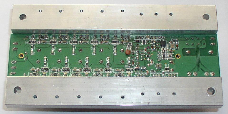
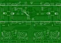
The "far side" ..... nice neat , compact SMD. Run dem babies , I wanna see a 120V p-p squarewave w/ 1uS rise
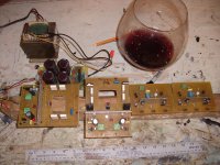
Oh , I feel so primitive I just had to enjoy a big glass of " vino" . I guess "no fine wine before it's time".... same with the DIY PCB's (below 1). First pair work fine , but have a slight thermal "issue" (but not a burning amp). Hopefully, this pair will work as good as they sound (thermally). I must fill that glass half way up to be truly subjective.
PS - PCB's are:starting left.... 2 X nikko PB120's (corrected version) and 2 X EX1.2 voltage stages (goldmund inspired). 1st PB120 is powered to test cap MUX'es. (below 2/3) the AX - being abused at 10Khz 60V p-p. 
OS
Oh , I feel so primitive I just had to enjoy a big glass of " vino" . I guess "no fine wine before it's time".... same with the DIY PCB's (below 1). First pair work fine , but have a slight thermal "issue" (but not a burning amp). Hopefully, this pair will work as good as they sound (thermally). I must fill that glass half way up to be truly subjective.
PS - PCB's are:starting left.... 2 X nikko PB120's (corrected version) and 2 X EX1.2 voltage stages (goldmund inspired). 1st PB120 is powered to test cap MUX'es.
(below 2/3) the AX - being abused at 10Khz 60V p-p. OS
Attachments
The "far side" ..... nice neat , compact SMD. Run dem babies , I wanna see a 120V p-p squarewave w/ 1uS rise
Oh , I feel so primitive I just had to enjoy a big glass of " vino" . I guess "no fine wine before it's time".... same with the DIY PCB's (below 1). First pair work fine , but have a slight thermal "issue" (but not a burning amp). Hopefully, this pair will work as good as they sound (thermally). I must fill that glass half way up to be truly subjective.
PS - PCB's are:starting left.... 2 X nikko PB120's (corrected version) and 2 X EX1.2 voltage stages (goldmund inspired). 1st PB120 is powered to test cap MUX'es.
OS
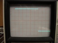
Nice score ostripper! Looking at the oscilloscope picture, my estimation is a rise time between 0.9 to 1.2μsec.
I would like to see a picture of your PCBs from the solder side.
FOS
still 1 board away.
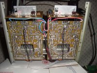
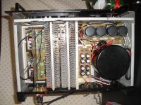
(below 1) is the solder side of the soon- to- go thermally unbalanced, but awesome sounding Nikko pb120's.
(below 2 - big board) is what I will have to do to get rock solid 60ma/device operation (fully separate heatsinks per amp). Nikko must of used ultra matched sankens + no base stoppers to get at least a close balance of idle current per device. Even in it's imperfect state , the amp can be pushed all day rail to rail with no issues. Unfortunately , I am a "perfectionist".
I will show the whole thing in a week with the "big board".
OS
Attachments
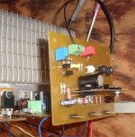
I found it curbside.
Fix it (schema attached) , it's a "pretty" receiver. Recap the power board , regrease the outputs (or replace with mj15003/4). If you were to make a new amp for it , design the PCB to be a exact replacement (no drilling). looks like the kenwood has a good, simple LIN topology EF2 AB amp with TO-3 outputs ... 55-0-55V PS ... typical.
OS
Attachments
Fix it (schema attached) , it's a "pretty" receiver. Recap the power board , regrease the outputs (or replace with mj15003/4). If you were to make a new amp for it , design the PCB to be a exact replacement (no drilling). looks like the kenwood has a good, simple LIN topology EF2 AB amp with TO-3 outputs ... 55-0-55V PS ... typical.
OS
Ostripper:
Thanks for the information. I looked at replacement capacitors when I first found it. I admittedly need to get better with a soldering iron. Don't want to burn down the house.
Time for "fine wine" (California ?)
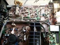
Finally it's done... What a PITA to redo a Nikko , no wonder others never concluded the job.
(attachment 1) is the wine /bottom , wired in the classic Japanese hi-fi style.
Yellow led is the main speaker relay board (protection to come soon)
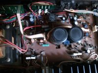
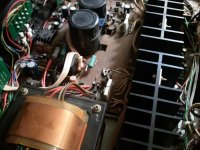
(Attachment 2) is the top view , 2 PS's (65-0-65V and 58-0-58V) , nice and tidy.
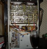
(Attachment 3 ) is how I got this far , had to make a special board or go for bust. Each amp has it own heatsink , 10C - 35C / 13-14mv (60mA - all OP devices) ... perfect Vbe. Sound is VERY detailed , quite the punch .. as well !!
OS
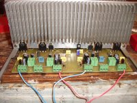
Finally it's done...
What a PITA to redo a Nikko , no wonder others never concluded the job.(attachment 1) is the wine /bottom , wired in the classic Japanese hi-fi style.
Yellow led is the main speaker relay board (protection to come soon)
(Attachment 2) is the top view , 2 PS's (65-0-65V and 58-0-58V) , nice and tidy.
(Attachment 3 ) is how I got this far , had to make a special board or go for bust. Each amp has it own heatsink , 10C - 35C / 13-14mv (60mA - all OP devices) ... perfect Vbe. Sound is VERY detailed , quite the punch .. as well !!
OS
Attachments
That is very cool
I first heard the Nikko line in the 1980s, when I was in college. Good stuff. You've gone the extra mile on that amplifier, ostripper.
Hoya Fan
Finally it's done...
(attachment 1) is the wine /bottom , wired in the classic Japanese hi-fi style.
Yellow led is the main speaker relay board (protection to come soon)
(Attachment 2) is the top view , 2 PS's (65-0-65V and 58-0-58V) , nice and tidy.
(Attachment 3 ) is how I got this far , had to make a special board or go for bust. Each amp has it own heatsink , 10C - 35C / 13-14mv (60mA - all OP devices) ... perfect Vbe. Sound is VERY detailed , quite the punch .. as well !!
OS
I first heard the Nikko line in the 1980s, when I was in college. Good stuff. You've gone the extra mile on that amplifier, ostripper.
Hoya Fan
- Home
- Amplifiers
- Solid State
- Post your Solid State pics here