There's small problem.With high power,when bass kick,there's slow move of speaker cone,cca 1Hz.This will ocur on any trackWhat is problem,maybe my phone?Of course it works, it even works with BIGBT, CFP, lateral mosfets, triple emitter follower outputs, you name it. That's the one and only VSSA front-end enabling all these threads.
Well I tried firing up my boards today without much luck. The first board started smoking the two 10R resistors behind the 4007s. The second one didn't smoke anything but it is pulling 140ma on the positive rail and has -.545VDC offset. I didn't have time to trouble-shoot but will try to get to it tomorrow. Does anyone have a voltage chart made up for this circuit? At least a ballpark of what I should be seeing at each of the transistors would be a big help.
Thanks, Terry
Hi Terry,
I have the same experience as yours. The busted resistors are caused by incorrect VAS transistors position or placement. The DC offset can be adjusted by connecting a parallel resistor on 15k to reduce or increase the value. The resistor template in Shaan's PCB the "OFF1" and "OFF2" is reserved for this purpose. You can try 150k or 330k or some appropriate value as needed to reduced the DC offset.
Sounds good to me,
Let me know when you have more blank pcbs. If you have some now that would even better.
The input transistors yielded large amounts of matchable devices. Many between 400 and 410 and between 410 and 420. I bought 100 each PNP and NPN. They are all tested and sorted.
I did not record Vbe but I can re-run and try to match Vbe as well as beta.
I have much fewer Vas matches but I have enough for a trade. I will order a larger quantity now that I know some matches can be had.
View attachment 370266
I have started my Peeceebee. I am using Rev 1.3 of the VSSA schematic. Input transistors are KSA992/KSC1845. These are the only transistors that I could get to match.
VAS transistors are BD139-16/BD140-16. Again these are the only ones I could get to match.
The LATFETs are in hand but not yet connected. I just want to understand the front end and driver biasing before I proceed.
My voltages are +/- 15 on the proto board. I changed 15K to 5K. All other passives are as per the schematic.
2.8mA through the PNP emitter. 3.0 mA through the NPN emitter. I changed the 470 ohm resistors to 1k pots to set the VAS transistors. Stock 470 ohm resistors caused 50 mA in the VAS transistors. I am dialing the 1k pots for 100 mV across the 10 ohm resistors.
Transistor pairs match are 1% to 2% at 30V and 2 mA for inputs and 10 mA for VAS transistors.
Question: In the V1.3 schematic, what should be the DC voltage to ground at the capacitor pair that grounds the connection of 47 ohm and 15k resistor?
Comments are encouraged.
5k was too low. Ic input was 2.8 - 2.9 mA. Calculated that 6.2k is correct for 2.286 mA which is what the stock design at 35V and 15k calculates to.
I changed the 5k resistors to 6.2k and the input Ic is now 2.3 mA.
Next hook up the output LATFETs and check bias and offset.
There's small problem.With high power,when bass kick,there's slow move of speaker cone,cca 1Hz.This will ocur on any trackWhat is problem,maybe my phone?
My amateur guess is thermal tracking problem. Are your input transistors glued together?
Second guess would be instability. Have you put a DMM on bias points and watch for drift?
Hi Acca, i guess this is problem:There's small problem.With high power,when bass kick,there's slow move of speaker cone,cca 1Hz.This will ocur on any trackWhat is problem,maybe my phone?
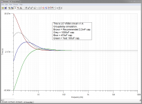
You get subtones delivered before the audioband 20-20K, about 64ms before audioband arrives. It is because you use only 100uF cap in feedback position, least recommended = 1000uF but better get 2200uF, it only needs to be 6,3V because DC/AC standing there is about 0.85V/2,44mV.
I attach simulation with different caps for graphic view.
And hi SHAAN been following this thread long, great stuff you have here, i just got modules from Andrew yesterday so start with that version first.
Regards Ricky.
Attachments
Last edited:
QOUTE post #1186:
Hi Again
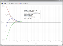
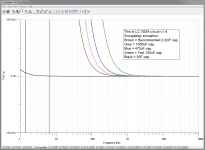
If someone is interested i attach two more images of groupdelay coursed by this cap in circuit.
To show what happens if you put one 35F/2,7V cap in there. If you are high end freak or have sound studio it would be preferable for precision.
I will try it later with this huge storagecap, but drawback can be if it has huge induction too then high band gets lost or circuit can be unstable.
First picture is same as post #1186, but with 35F cap plot, and second picture is zoom in to 0,1ms, where even 2,2mF is little bad looking.
Regards Ricky
Hi Again
If someone is interested i attach two more images of groupdelay coursed by this cap in circuit.
To show what happens if you put one 35F/2,7V cap in there. If you are high end freak or have sound studio it would be preferable for precision.
I will try it later with this huge storagecap, but drawback can be if it has huge induction too then high band gets lost or circuit can be unstable.
First picture is same as post #1186, but with 35F cap plot, and second picture is zoom in to 0,1ms, where even 2,2mF is little bad looking.
Regards Ricky
Attachments
Last edited:
Since the feedback is effectively two parallel feedback circuits, a difference in the resistors will have an effect (I am sure Shaan will correct me if I am mistaken about that).
No mistake. Small difference in this symmetrical network can indeed increase even order distortion and decrease PSRR. If someone has an extremely low ripple PS like your cap-mult then this characteristic can be used to simulate an SE amp, tested.
Well I tried firing up my boards today without much luck. The first board started smoking the two 10R resistors behind the 4007s.
Good call Pete. I just went and checked and on the one that smoked the 10Rs the ;BD 139 and 140 are swapped.
Hi Terry.
Also, make sure the VAS transistors have their metal backs facing the input side.
...The second one didn't smoke anything but it is pulling 140ma on the positive rail and has -.545VDC offset...
Iq seems okay.High DC offset is possible with unmatched components. It can be easily dealt with by adding the 'OFF' resistors.
This brings up the next issue. You mention adjusting the bias. How do you do that on the Shaan boards when there are no pots?
The resistor sourced VSSA that we are building has its input and VAS bias directly dependent on the PS voltage. So if you measured 10mA at +-15V then at +-30V it will double. Rule of thumb is to calculate a current source resistor value that gives an input bias of ~2mA at the highest PS voltage you are going to use. With +-35V it is 17.5K. If that is your PS voltage then install 18K in their place first (15K won't make too much of an increase in current either so should be okay too). This will make sure the input and VAS don't blow up at any PS voltage upto the maximum.
Check the VAS bias, if too low then replace the resistors with the next lower value, both at a time.
Utilizing the "OFF" resistors:
When you get a bias of about 10 to 15mA, check the offset. If it's positive then install a high value resistor to the positive "OFF" space, if negative then to the negative side. Please remember that increasing current in one polarity will drift the offset to the opposite polarity. As mentioned in the first post, almost always a resistor between 100K to 1Meg will be needed to be placed at any one of the "OFF" spaces. That said, both might be used to tame a wild-type offset to zero. For example, if placing a 220K in one side seems to null the default offset and also drift it too much beyond 0V to the opposite polarity then a 470K placed at the other empty "OFF" space will almost certainly bring it vary close to zero. Yes, there might be some experimentation necessary to set it up right, but hey, we're in the DIY forum.
...great stuff you have here...
Hi byrtt.
That's coz lots of passionate, kind and helpful guys here. Combined effort.
Thanks
shaan
No mistake. Small difference in this symmetrical network can indeed increase even order distortion and decrease PSRR. If someone has an extremely low ripple PS like your cap-mult then this characteristic can be used to simulate an SE amp, tested.
Hi Terry.
Also, make sure the VAS transistors have their metal backs facing the input side.
Iq seems okay.High DC offset is possible with unmatched components. It can be easily dealt with by adding the 'OFF' resistors.
The resistor sourced VSSA that we are building has its input and VAS bias directly dependent on the PS voltage. So if you measured 10mA at +-15V then at +-30V it will double. Rule of thumb is to calculate a current source resistor value that gives an input bias of ~2mA at the highest PS voltage you are going to use. With +-35V it is 17.5K. If that is your PS voltage then install 18K in their place first (15K won't make too much of an increase in current either so should be okay too). This will make sure the input and VAS don't blow up at any PS voltage upto the maximum.
Check the VAS bias, if too low then replace the resistors with the next lower value, both at a time.
Utilizing the "OFF" resistors:
When you get a bias of about 10 to 15mA, check the offset. If it's positive then install a high value resistor to the positive "OFF" space, if negative then to the negative side. Please remember that increasing current in one polarity will drift the offset to the opposite polarity. As mentioned in the first post, almost always a resistor between 100K to 1Meg will be needed to be placed at any one of the "OFF" spaces. That said, both might be used to tame a wild-type offset to zero. For example, if placing a 220K in one side seems to null the default offset and also drift it too much beyond 0V to the opposite polarity then a 470K placed at the other empty "OFF" space will almost certainly bring it vary close to zero. Yes, there might be some experimentation necessary to set it up right, but hey, we're in the DIY forum.
Hi Shaan,
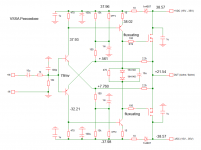
Thanks for the long, detailed explanation. I fear I have a bad device or two but to be honest, these poor little boards may not take to many more changes. I spent most of the morning trying to find the problem but now my head is filled with smoke. I have created a schematic that I will post below with the voltages I read. All are measured to ground. I am getting about +22V offset at the output. The collectors of both VAS transistors fluxuate around 0-300mv. When I just touch the DMM probe to them, the DC offset drops to 100mv. As soon as I release it the offset climbs back up to 22V. Weird. Anyway, hopefully one of you can take a look at the schematic and tell me where to look.
Thanks
Attachments
Is this one board, or are they both acting the same?
First I would lower the voltage (with your Variac), because less damage is likely to result at 15-20 volts. Then you can investigate more.
If the output voltage changes when you touch a probe to one of the VAS transistor leads, it may that you are reading the output of a circuit which is oscillating. (When you touch a probe to one of the VAS transistors, you may add just enough load to stop the oscillation.)
It is working
DC offset was -1/2V. I placed various resistors across the 6.2k resistor on the neg side until I obtained below 20 mV offset.
Mostly I wanted to verify the semiconductors before I committed the parts to a PCB.
I think my imbalance may be crappy resistors. I need to order some precision resistors for the soldered version.
I set VAS current above 10 mA and LATFETs above 100 mA. I am looking forward to having one connected to a scope so that I can start adjusting for minimum distortion.
Attachments
I have created a schematic that I will post below with the voltages I read.
Hi Terry.
Check the NPN input and PNP VAS transistors. Looking at the voltages I think one or both of them are either malfunctioning or just dead to an emitter-collector short-circuit. I particularly suspect the BD140.
What Pete said about oscillation is also a possibility, and faulty components can introduce a plethora of mysterious problems.
Sorry guys, I shouldn't bother you with this. It was mainly something to do while I waited for the rest of my Honey Badger pars. It looked like it would be fun and I had most of the parts in my parts drawers. I'm not sure I want to go through the work of fixing it when I am planning to build a nice one once Pete is ready to order more boards. (hint, hint) I may toy around with it some more to get a better grasp for when I build the next, but I'm not into trying several different parts until it works. I should have know when I first saw there were no pots that Bias and offset were likely going to be tricky to get right.
Hi woofertester.
Congrats. I love the noodlework!
Lookin' forward for more...
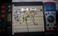
Its a laptop amplifier. I did a lot of the wiring sitting in an Ikea chair. The breadboard is self contained +/- 15V. I don't have to be anchored to my power supplies in my workshop.

Yeah, I might pull the transistors and test all of them. I probably hurt something when I got a couple things in backwards. This is a pretty simple layout. Even if I hurt the foil it won't be hard to run some jumpers. I am looking forward to building one on sanitary boards. These were a bit of a mess from the start. It was even difficult to do the drilling with the poor results I got from the transfer. Compound that with no silkscreen and I just made too many mistakes. I'll probably keep tinkering with them. I had better read through the entire thread. Seems there were changes along the way that I didn't know about. I'm sure I will learn something new before I'm done.
Blessings, Terry
Blessings, Terry
- Home
- Amplifiers
- Solid State
- PeeCeeBee