+/- pwr runs on opposed edges of the board is one of my gripes - really the worst for Class AB
+/- pwr trace should be on top of each other - as close to common centroid design as possible so that the "half wave rectified" currents magnetic fields "add up" to reflect the mostly linear load current
with pwr gnd/speaker out also nearby the fields even cancel to a degree
I wouldn't put the output inductor on the board - open cylinder solenoid coil radiates mag field badly too - hang them from the speaker terminal
how are you mounting to heatsink? aren't the MJL TO-264 flat plastic packages - not TO-3 metal cans your layout appears to show
do the boards have to be so small - hobby builds don't have the mass market price pressure, can improve some layout issues with added empty board space
thinking about multichannel operation - if you have a preamp/input buffer board then you could make the amp circuit front end a differential receiver to reject pwr gnd common impedance noise
I would always use the "beta enhanced" VAS today with some variant of 2-pole compensation given the design info we have - at least make it board stuffing option
Last edited:
I'm not entirely sold on the cancellation of the fields produced by the power supply traces, they occur at different times and therefore are not in exact opposition. I had entertained the idea of feeding the DC supplies directly to the metal mounting flanges of the outputs and just 'fingering in' the power to the rest of the circuit. I had also entertained the idea of putting the coil off board at the speaker terminal but felt I wanted a sort of all-in-one PCB. The emphasis I put on this one was on improving my grounding scheme.
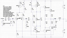
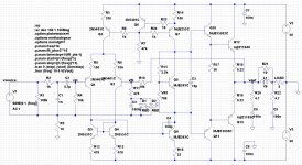
The devices listed on the schematic are what I had in the library for simulation purposes that were close to the MJ15003/15004 or MJ15024/15025 that I have handy. The outputs will be TO-3 metal cans. The small signal will be 2N5551 and 2N5401 and there are some other options in my parts box for drivers, VAS and CCS but the drivers will be TO-220 and VAS/CCS will be TO-126 or TO-225.
This is a rebuild of a much earlier project (like over 10 years ago) and I wanted to improve it some but would like it to retain the same dimensions, hence the rather small board. Also I can etch two from a standard 6"x4" pre-sensitized piece of board. For a true clean slate design the board would be probably be much larger. Attached is the old artwork from well before I knew better (note also that the circuit is not the same, nor the pinout of the small signal devices).
I did entertain the beta-enhanced VAS but the board was getting tight! TPC or TMC is also definitely recognized as having beneficial properties and again the real estate I was hoping to use was getting tight.
Thanks for the input.
Attachments
Some discussion of how to avoid the "opposite sides of the board power layout" that JCX (and I) dislike starts here.
Best wishes
David
Best wishes
David
Some discussion of how to avoid the "opposite sides of the board power layout" that JCX (and I) dislike starts here.
Best wishes
David
According to that discussion, I am trying to layout the PCB for my TT amp were big and small C multipliers are on the same board with the amp. On the attached PCB I started the layout and the OPS and plus side C multipliers are on. I have big problem how to layout the output and I can not find good enough solution for that part according what Charry suggests http://www.diyaudio.com/forums/soli...one-seen-front-end-before-92.html#post3164957.
dado
Attachments
![DADO-TT-TRIPLE-MPSA18-Cmult-small-b.LAY].jpg](/community/data/attachments/295/295734-d222c177bad97efce23f6a6291832e04.jpg)
I'm working on rearranging things a little, but I'm not fast like Alex MM, so I'll have something to show shortly to see what folks think. A short synopsis will be delivering the PSU rails directly to the TO-3 mounting flanges and fingering out to the low current areas on the PCB from the outputs.
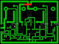
Does the grounding scheme in post #40 look OK? I was shooting for star-on-star with the audio star isolated by a 10 ohm resistor from the main ground on the PCB.
Does the grounding scheme in post #40 look OK? I was shooting for star-on-star with the audio star isolated by a 10 ohm resistor from the main ground on the PCB.
never drop the leading zero of values <1........ Any constructive comments or criticism welcome.
eg 0r22 or 0.22 is much less ambiguous than .22
never drop the leading zero of values <1
eg 0r22 or 0.22 is much less ambiguous than .22
Yes, this is true. I'll work on making component markings more succinct. Good tip for everyone, thanks.
So here's a version that has no large high current traces on opposing edges of the PCB, fusing will be off board on the PSU instead. Some components are a little better spaced and more distance between many of the traces. Any comments? Better or worse than the one on post #40 and why?
Attachments
look at the length of the route from V+ through C7 to Power Ground and then back to V- thro' C8. That route has to pass transients approaching and maybe even exceeding tens of MHz.
The total route length should be <20mm and preferably <10mm.
To achieve this the Power Ground must be located between the V+ & V-
Speaker Ground/Return does not need to be on the PCB.
The output R//L of the Thiele Network does not need to be on the PCB.
I believe they are both better located off PCB.
Add multiple Pin Pitch options to as many caps as you can manage in the layout as is.
Last edited:
look at the length of the route from V+ through C7 to Power Ground and then back to V- thro' C8. That route has to pass transients approaching and maybe even exceeding tens of MHz.
The total route length should be <20mm and preferably <10mm.
To achieve this the Power Ground must be located between the V+ & V-
Speaker Ground/Return does not need to be on the PCB.
The output R//L of the Thiele Network does not need to be on the PCB.
I believe they are both better located off PCB.
Add multiple Pin Pitch options to as many caps as you can manage in the layout as is.
OK, I was concerned about the bypass returns being so long. Could a separate ground be provided solely for the bypass return or is it best fed to the board's main star? Relocating the main star will require a complete redo. Are you referring to the total path from +V through C7 and C8 to -V being under 20mm or each rail through its respective bypass capacitor to ground being less than 20mm?
I understand the output inductor and speaker return can be located off board but aside from lost real estate is there any real disadvantage? That said the RC Zobel (C6 and R20) should remain local, correct?
Additional pin pitch options do make sense for a public consumption project. In this case, for this little project, I already have what I will be using, so the pitch is fixed at the moment.
All this said I'm seriously looking at scrapping the chosen board size and going with a larger PCB, but not just yet. This is to retrofit into a project I did over 10 years ago and would like to reuse the heatsink and not disturb the existing layout if possible.
Thanks for you input thus far. I'm slow with the artwork, I find I spend much time just looking and mentally routing and repositioning. I'll post some different options as they present themselves.
total length from V+ to V- via the HF decoupling <10mm. The MF decoupling route can be much longer maybe 50mm for total route. And yes, the decoupling Ground is actually the Power Ground. The HF decoupling Ground should be connected to the MF decoupling Ground and the ground from the PSU connects here. The speaker does not need to connect here. The Zobel does need to connect here. It too passes HF and it too needs a very short route.OK, I was concerned about the bypass returns being so long. Could a separate ground be provided solely for the bypass return or is it best fed to the board's main star? Relocating the main star will require a complete redo. Are you referring to the total path from +V through C7 and C8 to -V being under 20mm or each rail through its respective bypass capacitor to ground being less than 20mm?.............................That said the RC Zobel (C6 and R20) should remain local, correct?
the air cored coil should not be near iron components, maybe just as important, other sensitive audio components should not be near the field of the air core. If that is the case, then the coil and it's damping resistor need to be off PCB............is there any real disadvantage?
Once you have the HF & MF decoupling grounds connected and you bring power into this same Ground and also bring the Zobel capacitor to here as well there are only two other connections on the PCB that need referencing to the Power Ground. The Signal Ground isolating resistor comes here and other small current grounds come here.
In summary:
Locate the Power Ground right in the middle of the output stage and bring all the other connections to this location.
Don't spread the Ground around the PCB. I don't think that achieves any benefits. Guess what? That's the opposite to a ground plane. I have regularly argued against that unless you know how and why that plane is needed/works.
Last edited:
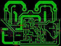
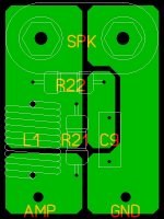
So I will move the output inductor and damping resistor to a separate board at the speaker terminals as shown. I then elected to make the output network a Pi network by following up the inductor with another Zobel, R22 and C9 on the revised schematic.
Attachments
So here's a version that has no large high current traces on opposing edges of the PCB, fusing will be off board on the PSU instead. Some components are a little better spaced and more distance between many of the traces. Any comments? Better or worse than the one on post #40 and why?
The bias is tracking the output transistors rather than the drivers. This is very strong tracking indeed. How would mounting everything on main heat sink work out ? So that all dies are almost at the same temperature together with the added benefit of higher hfe, although would this cause instability ?
The layout looks interesting and you have covered most issues although a few may need addressing
")
So I will move the output inductor and damping resistor to a separate board at the speaker terminals as shown. I then elected to make the output network a Pi network by following up the inductor with another Zobel, R22 and C9 on the revised schematic.
Mouting them off-board may be ok, however where is that gnd connection to speaker coming from
Assume you have large decoupling caps on board which you dont, assume that this is a multi channel system which you will tell us
Assume that due to the large onboard decoupling caps, there is a sizeable current running on the gnd about 4 A, assume that there is resistance between the star ground and onboard ground of about 0.15 ohms. What would be the voltage difference between the two grounds ?
Last edited:
The Speaker Return connects to the Main Audio Ground (MAG).
That MAG has connections running to>
1.) Signal Ground @ either the PCB, or at the RCA input.
2.) Speaker Return.
3.) Power Ground on the PCB.
4.) PSU Zero Volts.
5.) Chassis, either direct, or via a Disconnecting Network.
6.) optional auxiliary grounds/references.
That MAG has connections running to>
1.) Signal Ground @ either the PCB, or at the RCA input.
2.) Speaker Return.
3.) Power Ground on the PCB.
4.) PSU Zero Volts.
5.) Chassis, either direct, or via a Disconnecting Network.
6.) optional auxiliary grounds/references.
The design of a PCB I'm relatively new at. In the past I just connected everything that needed connected in what seemed to be the most logical fashion and it seemed to work. At this point I'm looking to learn a few tricks and up my skills in the PCB department. That is really to point of the thread, so I am going based on a relatively simple conventional design as the basis of my learning curve.
Thanks for the input so far and I'll continue to rework the design an post my progress. I'm not fast with the artwork, but I'm working on it.
Thanks for the input so far and I'll continue to rework the design an post my progress. I'm not fast with the artwork, but I'm working on it.
Ground loops can be a big problem in pcb design.
I laid out an audio mixer just as it came and when I got the pcb back there was loads of hum.
I relaid it out seperating the power supply ground from the rest of the circuit and there was almost zero hum. So using star grounds is a good tip. I have notcied a lot of amps have seperate power supply pcb's so perhaps they have coem across the same problem that I did.
- Home
- Amplifiers
- Solid State
- PCB Layout Process and Guidelines?