I tend to layout pcbs as they come from the schematic as items that are close to something else usually connect to them. Clearly edge connectors and output transistors need to go on the edges first.
Just as important as routing is design rules checking.
Clearance check.
Layers out of range check (dont want layer if dual layer board.)
Minimum via size check. (vias often have a minimum size for a pcb vendor. I always use 40 thou holes.
Continuity check, makes sure all tracks are routed and connected to corrent layers.
Integrity check, pcb should match the schematic, simple fact but vital.
You should also have done error checking on schematic, single ended nets, lines under pins but not connnected. Unconnected pin scan.
my 3 euro cents
amplifiers (and preamplifiers also ) are very often degraded or derated or whatever by the pcb ...the actuall circuit simulates wonderfull and when its made out is by far more worst ...
to design pcb for amplifiers there is a guideline and a few rools
--- decoupling has to take place close to outputs
--- small signal stuff has to be one one area close probably featuring ltp thermal junction
---rails have to be as small is possible
--- ground trace more or less the same
--- starground will be also e a bless
--- zobel has to be far away from input
--- curent mirrors and sources have to be close to the divisions that support
--- miller caps are to be located close to the related transitors
--- management and distribution of earth is a trick
--- ground plane can be twice as worst
--- heatsinks for some transitors might consume area
--- and probably afew others i missed ....
Dont fool your shelf !!!! NO-ONE can make a pcb that can follow all these rules in a single layer ( even for an amplifier that has very low part count )
messing up with a dual layer can be also complicated since its messing up with ground plane or managment and distribution of earth and if not designed properly will/can introduce capacitance and inductaunce between layers ...
in real life one could go for small amplifier /single layer aprx. >100W try to follow as many of the rules above .
aim of the above is to low distortions as much is possible .. the pcbs of this style cannot be comercially produced or assemblied fom robots ... the comercial designers skip quite many of these rules to make there machines able to be massivelly produced and more cost effective ...
redesign of pcb and cable rooting of any comercial amplifier will increase the cost of production 3-4 times but also low the distortion and crosstalk issues to minimum ...
as about Alex mm pcb sorry to say is that i have never seen anything trully inovative from him ... eventhough he is a very hard working guy for free and for the family of the diyaudio .... still he made a pcb once and all his other pcbs is based on the same patern ...
there is other ways to do things ( dont have to be better or worst ) simply they need to e more inovative ...
Joke :
i am curently working on the P3A ( been doing so for 4-5 years ) had a friend asking me to design a couple of pcb based on the schematic of the P3A but designed length wise to be possible to fit on the back of a specific speaker it could be only 4 cm wide and long something between 20-25 cm ...done it in a dual leyer but for some reason the P3A never sounded as good as the original pcb made eventhough parts where exactly the same .... any ideas ? )
Last edited:
Good advice above, I'll just add one thing. Don't settle on the first layout that looks good. If you leave a design for a day or so, then come back to it fresh, you will often notice little things you can change to optimise the layout, or even big things that mean you have to rip up part of the layout and completely redo it. Don't be afraid to do so.
You're not wrong on that Al! I'd worked and worked on the layout for my regulated supply (slightly different because it is verro board) and reached a point where I just didn't think I could improve it any more.
I left it for a few months (not advocating that long!) and came back to it and have made some major revisions for the better. Still probably not 100% but a break certainly can give you a new perspective.
Tony.
I left it for a few months (not advocating that long!) and came back to it and have made some major revisions for the better. Still probably not 100% but a break certainly can give you a new perspective.
Tony.
Hugh,
this "bloody" design (drawn with Microsoft Paint, disregarding any theoretical advice - representing Carlos' DX Blame ES) took me 50 hours.
http://www.abload.de/img/kk001ejal.jpg
The result has been a "rock-stable" AMP, "playing to pour its heart out to you."
http://www.abload.de/img/shootout0179khh.jpg
and has been unmatched for quite a long time (in my ears, according to several listening tests with my AUDIO-friends, "shoot-outs with famous brands", ...).
Theory is on the one side - real life may differ from it.
Remember: we do not have any GHz-signal acting like an antenna on an AMP's PCB, we do not have any µV - signal, being crossed / paralled by a Kilo-Volt-signal, ...
This is my experience.
Best regards - Rudi_Ratlos
this "bloody" design (drawn with Microsoft Paint, disregarding any theoretical advice - representing Carlos' DX Blame ES) took me 50 hours.

http://www.abload.de/img/kk001ejal.jpg
The result has been a "rock-stable" AMP, "playing to pour its heart out to you."

http://www.abload.de/img/shootout0179khh.jpg
and has been unmatched for quite a long time (in my ears, according to several listening tests with my AUDIO-friends, "shoot-outs with famous brands", ...).
Theory is on the one side - real life may differ from it.
Remember: we do not have any GHz-signal acting like an antenna on an AMP's PCB, we do not have any µV - signal, being crossed / paralled by a Kilo-Volt-signal, ...
This is my experience.
Best regards - Rudi_Ratlos
Hi,
I work with the software Kicad. It is open source and is also suitable for professional printed circuit board manufacturing.
The advantage over sprint layout is that you can go directly from schematic to layout. The progam detect faulty connections in the layout immediately. Since I use Kicad I've never produced a bad layout. If there were errors, they were already in the schematic.
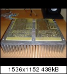
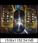
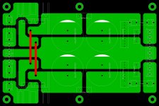
Here's my the most power-size-concentrated module I've ever made, ProJet Power Module mono PCB from few years ago. It was more a tour de force than possibly commercial success but nevertheless I made it and it works properly according to specifications. Ten output devices (two are drivers) on such small area is quite an achievement as to some pro's opinions. Tracks are short, well routed and the board has some 70um base + cca. 200um extra copper thickness, double layer with metallized holes, all in white colour. 
Attachments
hi jkuetemann,
Here's my advise.
1. Read as many related posts as possible, all the information has be posted before, over and over.
2. Just do it and get it finished. It will never be "perfect" but learning from you own experience is invaluable.
3. Do not ask too many questions, you will only get 15 contradictory replies that will confuse the issue and prolong the project.
4. All (most) of us post information based on anecdotal evidence. Amp A sounds better than Amp B, arh... it must be because the PCB is red not green.
regards
hi jkuetemann,
3. Do not ask too many questions, you will only get 15 contradictory replies that will confuse the issue and prolong the project.
My advice comes from 30 years experience of pcb design.
It also comes from 20 years of writing and improving pcb cad design software.
Error checking is absolutely vital and I have concentrated on this.
My advice comes from 30 years experience of pcb design.
It also comes from 20 years of writing and improving pcb cad design software.
Error checking is absolutely vital and I have concentrated on this.
hi nigelwright7557,
I tried to PM you and this reply doesn't add value to the thread, but it seems you have PM turned off.
I have read lots of your posts over the years and have great respect for your knowledge and skills, not to mention your keenness to pass on your experience. I am also envious of your software writing skills, that would be perfect, to have such control of the design process. I wasn't having a go at anyone.
Yes, error checking is absolutely vital. I won't look at posted PCBs in detail unless the schematic is also posted. IMHO, software that doesn't have forward and backward annotation is next to useless but I have seen people do the job with MS Paint but who am I to say this is the wrong approach for them.
regards
hi nigelwright7557,
I tried to PM you and this reply doesn't add value to the thread, but it seems you have PM turned off.
I am also envious of your software writing skills, that would be perfect, to have such control of the design process. I wasn't having a go at anyone.
regards
According to CP my pm is on.
You can download a copy of visual c# express and start writing your own pcb software. C# is very powerful for programming and also is great for pcb graphics for pads tracks text etc
When I first started I had to write all my own graphics routines right down to plotting points, tracks, pads text etc. and that was all done in assembler writing directly to the pc screen bitmaps !
I developed my software while using it, as I found a need for a new function e.g. back annotation then I would add it.
My software is flogged to death and has around 500 users so I get to know of bugs very quickly. If anyone finds a bug then I fix it and immediately send them an update. Other companies just add it to a "to do" list for the next revision.
Last edited:
According to CP my pm is on.
Sorry to reply to myself but I fixed the PM, I had opted to only let moderators PM me.
Pcb design is a form of industrial art with strong technical input. You learn by doing, then being coached by an experienced person. It's not easy and takes years to perfect, and even then there are always criticisms. The advice given here is excellent.
Nigel, how do you create a thermal relief pad in Protel 1.12? I realise you may not know, but it's driving me crazy and any advice gratefully received,
Cheers,
Hugh
Nigel, how do you create a thermal relief pad in Protel 1.12? I realise you may not know, but it's driving me crazy and any advice gratefully received,
Cheers,
Hugh
Last edited:
Nigel, how do you create a thermal relief pad in Protel 1.12? I realise you may not know, but it's driving me crazy and any advice gratefully received,
Cheers,
Hugh
Not sure about Protel but my software automatically creates a powerplane with relief for pads and tracks unless the track net is connected to the powerplane net.
I had good results as the designer, sitting with the contract PBC layout "jockey" - I could guide parts placement, highlight sensitive nodes, runs, voice concerns on power distribution - but he could run rings around me in implementaiton choices, running the sw
when on my own rats nest with rubber banding, starting with absolute constraints on power distribution/seperation from sensitive circuits - a willingness to start over when finding myself "cornered" seem most valuable
don't forget that as a hobbyist jumpers, above board bus bars, dropping soldered input, output or even power (twisted pairs) into the middle of the board can be practical where mass manufacture may prevent such "shortcuts"
Last edited:
Don't forget that as a hobbyist jumpers, above board bus bars, dropping soldered input, output or even power (twisted pairs) into the middle of the board can be practical where mass manufacture may prevent such "shortcuts"
Yes, I must remember these things as well. I'm planning on constructing my boards at home, so combinations of these techniques are allowable. DIY has a certain flexibility in implementation you don't get in mass manufacture. I appreciate the input that has been provided. I will also continue to 'study' some of the more popular / successful projects here to see how the more experienced have chosen to approach the task.
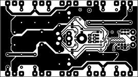
First off, sorry about reviving an old thread of mine but since the content is relevant I figured better to continue with this one than start anew.
I'd like some peer review related to the PCB layouts more so than the schematic. I'm looking for gross layout problems or outright errors that I may not have seen. I am also interested in the finer points as well. Any constructive comments or criticism welcome.
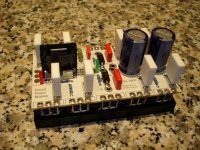
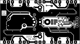
I'd like some peer review related to the PCB layouts more so than the schematic. I'm looking for gross layout problems or outright errors that I may not have seen. I am also interested in the finer points as well. Any constructive comments or criticism welcome.
Attachments

- Home
- Amplifiers
- Solid State
- PCB Layout Process and Guidelines?