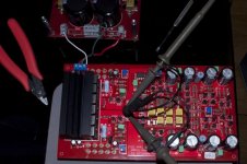
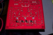
Pictures of the right channel board (top side), and left channel board (reverse side). The reverse of the right channel board is identical. Yes I was carefully with the pinout of the ZTX devices.
As you can see, I was able to replace Q102 etc without removing the heat sink. This is a nice design and I am keen on solving this problem.
B.t.w. I am running the PS without any load.
Should I replace Q105 and Q205 (currently high hFE) by lower hFE ZTXs?
Suggestions would be appreciated… Many thanks in advance !
Pierre
Attachments
Thank you for asking.Do you have the compensation caps mounted?
Yes, between the base and collector of Q102, Q104, Q202 and Q204. This is version R3 of the pcb so there is no dedicated footprint for them: I soldered them on the pins of the transistors on the bottom side of the board (a pain!). 3300pF on Q102 and Q202 (the middle two transistors in the right-hand picture of the previous post) and 680pF on Q104 and Q204.
Should I try different values for the compensation caps?
Or different transistors? I started with BC327/337 having hFE over 500, then BC327/337 having hFE around 400, and currently ZTX550/450 having hFE between 150 and 200. The next step could be MPSA92/42 with lower hFE still.
Pierre
Last edited:
The problem in the right channel board is a tough nut to crack… I've tried increasing the b-c compensation caps in the CCS up to 12 nF, then tried the same in the CVS, but it did not help much...
What I am thinking next is playing in the shunt, starting with Q105. Since changing Q107 worsened things, perhaps the BC337-40 in Q105 is "too nervous". (I'm guessing here). Will try a ZTX450, and if need be, a small cap between base and collector.
A question: Performance-wise, is there a preferred hFE value for Q105 ?
Pierre
PS On the bright side, I'm understand the circuit a little bit better every day .
.
What I am thinking next is playing in the shunt, starting with Q105. Since changing Q107 worsened things, perhaps the BC337-40 in Q105 is "too nervous". (I'm guessing here). Will try a ZTX450, and if need be, a small cap between base and collector.
A question: Performance-wise, is there a preferred hFE value for Q105 ?
Pierre
PS On the bright side, I'm understand the circuit a little bit better every day
.It strikes me that it is illogical to simply swap out components on one faulty board when the other (identical?) board appears to work correctly. Unless a component has gone off tolerance limits or is otherwise damaged [or indeed failed] at best all you may succeed in doing is altering the board for a 'good enough' result. Far more logical is to test every aspect of the board from input through to output and compare the results with those, executed identically, for the 'good' board. This is a 'big' build and not cheap...it is worth the effort to get it right rather than just patched-up.
It is sad that those posters who really know this design have been unavailable to suggest possible causes.
It is sad that those posters who really know this design have been unavailable to suggest possible causes.
Last edited:
Thank you Brian.
Prompted by your good suggestion, I meticulously probed both boards and compared measurements to each other and to the reference voltages of the manual. Everything measures within 100 mV of the reference voltages EXCEPT in the shunts, where the differences can be explained by the jets used (J310 or J113) and the Vgs of the 610 and 9610 Mosfets.
I did find a problem: unfortunately in the better one of the two boards!!! The Mosfet in the positive regulator of the left (good) board has a Vgs of only 3.2V. This leaves only 0.5 V for Vds of the J310 which likely prevents it from working properly as a current source. Because the output voltage goes down slowly as the board warms up, I suspect the disappearance of the oscillations is not evidence of stabilization, but rather of Q107 starting to choke and the regulator weakening… I know what to do: change the J310s for J113s and test again.
Just to be on the safe side, I increased the gate resistors on the Mosfets of the right board from 100 ohms to 221 ohms because Mosfets are known to be prone to oscillation. But this made no change at all.
Pierre
I am not competent to offer any further suggestions Pieere, however I am sure that a few of those who are competent will soon come up with more helpful suggestions, if not a full pinpointing of the problem. [Joachim has recently said that he is very busy with something else].
Are you using Calvin's buffers in your build?
Are you using Calvin's buffers in your build?
Pictures of the right channel board (top side), and left channel board (reverse side). The reverse of the right channel board is identical. Yes I was carefully with the pinout of the ZTX devices.
As you can see, I was able to replace Q102 etc without removing the heat sink. This is a nice design and I am keen on solving this problem.
B.t.w. I am running the PS without any load.
Should I replace Q105 and Q205 (currently high hFE) by lower hFE ZTXs?
Suggestions would be appreciated… Many thanks in advance !
Pierre
Hi Pierre, changing Q105 and Q205 should not make much of a difference. Are the collector voltages of Q105 ad Q205 at around +/-15V alright?
Can you please remove C104 and C204 just for a moment, to see if it makes any difference?
Guessing at this point.... lets see - so far we have resolved every single oscillating board, and we will solve this riddle as well!!
Are you using Calvin's buffers in your build?
Not yet. I have them and intend to use them, but for now I am postponing the mod so I can debug my build in stock form before adding more complexity.
Pierre
Hi Pierre, changing Q105 and Q205 should not make much of a difference. Are the collector voltages of Q105 ad Q205 at around +/-15V alright?
Can you please remove C104 and C204 just for a moment, to see if it makes any difference?
Guessing at this point.... lets see - so far we have resolved every single oscillating board, and we will solve this riddle as well!!
Many thanks in advance for your help
.For the left board, which is on the bench, the collector voltage of Q105 is 15.07V and that of Q205 is -13.66V. For the right board, they are 14.35V and -13.68V.
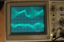
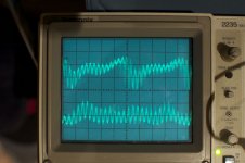
Here's a photo before removing C104 and C204. 50mV and 0.5us per div, with BW limit (20MHZ).
Attachments
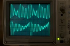
Right channel, after changing the two J310s for J113s, and their Rgs from 3.3K to 1.0K. Current through the resistors is 1.15 mA. Scope now set at 50 mV per division. The time scale is unchanged at 0.05 us.
Sorry for the delay, I have been away a bit
. The correct JFet to use is the J113 and the current set should be (about) 1mA. This should result in a Vds of about 1.5 Vols.These are the most important/relevant messages regarding PSU and Pre-Reg.
- Mpp #4375 PSU-pre-regulator.
- Mpp #4610 V2 Schemas UPS and Amp.
- Mpp #6506 CCS fine-tuning.
- Mpp #6462 PSU with my notes.
- Mpp #6809 Do not try to feed the CVS of the CCS of the shunt with a regulated power supply.
- Mpp #7127 More about transformer selection.
- Mpp #7635 Single and dual transformer wiring (also corrected drawing) (See also #7733).
- Mpp #7733 Grounding (PSU, RIAA and Player).
- Mpp #7810 35V PSU for the CroMagnon.
- Mpp #7830 The PSU explained.
- Mpp #8386 My resistor recommendation’s.
- My Paradise #56 PSU Noise.
- Masterpiece #951 That's not a PSRR test (it's a CIR test)
- PradiseBuilders #13 Schema's and assembly guide.
- PradiseBuilders #155 Vdc input voltage minimum simulated.
- PradiseBuilders #970 PSU oscillates; posible solutions?
- PradiseBuilders #983 Compensating the PSU for oscillations.
- PradiseBuilders #1173 Fixing oscillations (up to #1182).
- PradiseBuilders #1322 Fuse .
- PradiseBuilders #1387 Updated Paradise R3 assembly guide (Also German).
- PradiseBuilders #1403 Capacitors bad vs good.
- PradiseBuilders #1593 PSU Power Transistor selection.
- PradiseBuilders #1644 PSU Output Impedance.
- PradiseBuilders #1680 PSU Power Supply Suppression Ratio(PSSR).
- PradiseBuilders #1772 NJF selection for the PSU.
- PradiseBuilders #1887 Empirical NJF Rgs determination.
- PradiseBuilders #2127 More about the PSU fets (J113's etc).
- PradiseBuilders #2969 About the Paradise PSU using Calvin buffers.
- PradiseBuilders #3134 More ESR confusion .
Pictures of the right channel board (top side), and left channel board (reverse side). The reverse of the right channel board is identical. Yes I was carefully with the pinout of the ZTX devices.
As you can see, I was able to replace Q102 etc without removing the heat sink. This is a nice design and I am keen on solving this problem.
B.t.w. I am running the PS without any load.
Should I replace Q105 and Q205 (currently high hFE) by lower hFE ZTXs?
Suggestions would be appreciated… Many thanks in advance !
Pierre
No need for high Hfe devices in the PSU anything above 200 is file 300 to 400 is best (I think).
Many thanks in advance for your help
For the left board, which is on the bench, the collector voltage of Q105 is 15.07V and that of Q205 is -13.66V. For the right board, they are 14.35V and -13.68V.
Here's a photo before removing C104 and C204. 50mV and 0.5us per div, with BW limit (20MHZ).
Most of the boards that I did have, and that oscillated, needed replacement of the power transistors. What power transistors are you using (D44H11/D45H11?). Some of the links that I just posted do discuses the power transistors.
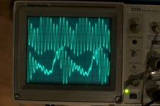
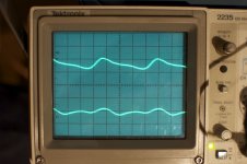
Now after removal of C104 and C204. 20mV and 0.05us per div. Looking better!
The measured output voltage is 18 Volt and can be adjusted using the potentiometer? Over what range can it be adjusted?
What power transistors are you using (D44H11/D45H11?).
Yes. Mouser Part # 511-D44H11 from China and Mouser Part # 511-D45H11 from Morocco. Straight from the bag; I did not bother to measure hFE for these.
The measured output voltage is 18 Volt and can be adjusted using the potentiometer? Over what range can it be adjusted?
Yes, I can adjust output voltage between 17.5 and 19.2V. They start a little higher (18.5V) and settle down to 81.2V in a few minutes. All measurements and scope shots were made at +18.2V and -18.2V after warm up.
- Home
- Source & Line
- Analogue Source
- Paradise Builders