Yes I did leave out R15 and I followed the few changes on the last page of the assembly guide. I don't have any visible shorts, I'm sure.
How about the pin layout of the output transistors - it seems the 2SA1381 is not different from the Fairchild BD14016STU I used. I assume the side with the writing faces up?
Beside the BD140 I used Fairchild J107 and PF5102 so the whole pin layout stuff should not be a problem?
Best to check the datasheets to be sure you put them in the right way, these transistors are misleading....
Also, one more recent issue that came up: For the foil caps, the footprint on the PCB will allow putting 2.5mm / 5mm / 7.5mm / 10mm caps, however the 5mm caps have two possibilities to be put, one of which will not work however (the short-circuited one - you can easily see it on the PCB). But when you solder a 5mm cap in the "wrong" spot, chances are you are shortcircuiting the cap, which leads to high current consumption in the buffer. Does not seem to destroy it but obviously it won't work. So you may want to check your caps......
Thanks guys. The caps are built in correctly and I do not have any shorts on the heat sinks.
But I guess the fact that - for some reason - I have 200R trimmers instead of 2k's might be part of the problem.")
Should I expect anything to be damaged because of this?
Best Regards
Sven
But I guess the fact that - for some reason - I have 200R trimmers instead of 2k's might be part of the problem.
Should I expect anything to be damaged because of this?
Best Regards
Sven
Last edited:
Thanks guys. The caps are built in correctly and I do not have any shorts on the heat sinks.
But I guess the fact that - for some reason - I have 200R trimmers instead of 2k's might be part of the problem.
Should I expect anything to be damaged because of this?
Best Regards
Sven
Your dignity
After adjusting the buffer to zero offset everything seems to be in order except it takes about 20 seconds for the large groups of LEDs on the shunt to light up. Video here, the "clicks" are on/off and I'm measuring the offset of the buffer. The LEDs under the heat sink light up immediately.
Is this a problem?
Thanks
Sven
Is this a problem?
Thanks
Sven
Hi,
The current the circuit draws is rather defined in the upper half, namely R6.
R11 stes the overall current in the lower half.
R5 and R7 define how the overall current splits between the JFET path and bipolar path.
If the transistors are all matched perfectly, the Trimmer pot need to be set top 856Ohms (in parallel to R8a this results in 175Ohms, the sum of R1 and R2).
Turning the pot fully either way results in a dead short, or 198Ohms.
I assume that there is a strong asymmetry between the upper and lower half of the circuit, due to transistor mismatch, or maybe a wrong valued resistor.
Could You in a first instance measure the voltage drops over R6 and R11 and R5 and R7?
Also voltages over and resistances of R1+R2, rep. R8a||R8b.
Ideally those should be pairwise equal.
jauu
Calvin
The trimmer is just there for trimming output offset voltage.When I turned it completely the lights came up. Appearently the buffer pulls too much current in the "middle" setting
The current the circuit draws is rather defined in the upper half, namely R6.
R11 stes the overall current in the lower half.
R5 and R7 define how the overall current splits between the JFET path and bipolar path.
If the transistors are all matched perfectly, the Trimmer pot need to be set top 856Ohms (in parallel to R8a this results in 175Ohms, the sum of R1 and R2).
Turning the pot fully either way results in a dead short, or 198Ohms.
I assume that there is a strong asymmetry between the upper and lower half of the circuit, due to transistor mismatch, or maybe a wrong valued resistor.
Could You in a first instance measure the voltage drops over R6 and R11 and R5 and R7?
Also voltages over and resistances of R1+R2, rep. R8a||R8b.
Ideally those should be pairwise equal.
jauu
Calvin
Hi,
btw. after my sims the idle current through R6/R11 is ~70mA, much higher than required.
The following combinations of R6/R11 and R5/R7result in currents through R6/R11 - R5/R7 - Q1/Q4:
2R2 - 6R8
7.1mA - 64.1mA - 70.1mA
4R7 - 6R8
6.0mA - 41.9mA - 47.7mA
6R8 - 6R8
5.5mA - 32.3mA - 37.6mA
8R2 - 6R8
5.3mA - 27.9mA - 33.1mA
4R7 - 4R7
5.7mA - 46.6mA - 52.0mA
I´d rather choose one of the two combinations with same value for R5,6,7 and R11, hence 6R8 or 4R7.
>30mA is much more than sufficient for any load >1kOhm.
It reduces heat dissipation and leaves more current for the shunt regulator, which certainly improves that´s condition and performance.
jauu
Calvin
Could You in a first instance measure the voltage drops over R6 and R11 and R5 and R7?
Also voltages over and resistances of R1+R2, rep. R8a||R8b.
Ideally those should be pairwise equal.
Here we go:
Voltage over R5: 0,218V
Voltage over R7: 0,218V
Voltage over R6: 0,080V
Voltage over R11: 0,080V
Voltage over R1: 4,97V
Voltage over R2: 3,40V
Resistance: R1: 98,5R
Resistance: R2: 67,6R
Voltage over R8a||b: 0,836V
Resistance: R8a||b: 158R
New video about the current flowing after switching on. Starts with >70mA per side and after the 20 seconds it goes down to 28 (this is also when the lights on the shunts come up).
Hi,
I assume that the voltages over R1,R2 should read 0.437V and 0.34V, in sum 0.837V.
Which is very close to the voltage drop of 0.836V over R8a||R8b.
The resultant currents are:
I(R5,R7): 32.06mA
I(R6,R12): 36.36mA
I(R1+R2): 5.04mA
I(R8a||R8b): 5.29mA
All votages and currents match nicely.
So everything seems perfectly ok with the Buffer.
As there are quite a few large Caps in the Paradise and not much overhead current from the CCS left, the charging timeconstants get longer.
jauu
Calvin
Yes, its 0,* - sorry.
So nothing to worry about. Strange though that nobody else seems to have these issues. Can I be 100% certain that the shunt delivers enough current for both loads? I should probably change the load resistor of the shunt to 8,2 as suggested in the assembly guide and by others earlier...
Another questions:
I noticed the little heat sinks of my other buffer are a few degrees colder. I have only 0,168V over R5,7 instead of of 0,228V. Don't know why, i used exactly the same parts. Could that be a problem?
Many Thanks
Sven
Last edited:
Hi,
168mV over R5,R7 means 24.7mA into the emitters of the bipolars.
Are the voltage drops over R5 and R7 identical?
Lower voltage over R5 indicates to a lower base voltage of Q3, due to a lower current through R1+R2 and as such lower currents through the JFETs.
The drain current of JFET Q1 - besides the earlier mentioned ratio of R6 and R5- is basically the defining parameter here.
If the drain currents of the J1s between left and right channel differ, so will the currents through the bipolars and the overall idle currents of the circuits differ.
The function of the pot in the lower half serves exactly the purpose to trim the bipolar current, so that the summed current through R6, resp. R12 are equal.
This means that even if the currents through the R6s and R12s equal, that the current distribution in the JFET-paths and the bipolar paths may differ between upper and lower part of the Buffer as well as the left and right channels.
As only the lower part features the trim pot, there may occur inter-channel differences due to differing J1s.
You may want to check what the other voltages measure?
jauu
Calvin
Abraxas, I have the same issue too. On one channel it really takes a while before the positive LEDs go on. I measured the Input and Output voltages, and all is stable, no offset, so I leave it like that.
It actually is only there when the Calvin buffer is installed...without, all normal....
Rem
It actually is only there when the Calvin buffer is installed...without, all normal....
Rem
Help with PS please
Hi all
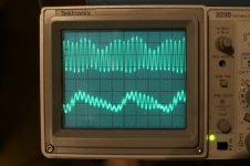
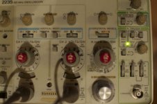
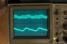
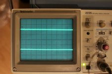
I have assembled two R3 boards and cannot get rid of oscillations in the power supply. The LEDs turn on, the voltage at the output is close to +18V and -18V. The current through the 3.3K resistor next to the J310 is about .75 mA. The positive and negative rails of both boards oscillate at a few MHz plus ringing in the tens of MHz.
Q102 and Q104 are high hFE BC337-40 from ON SEMI. Q202 and Q204 are high hFE BC327-40 from Fairchild. I have tried adding the film caps as is now recommended. This reduced the amplitude of the oscillations, but did not eliminate them. I added small resistors to the last filtering electrolytics (to lower ESR) without results.
The most significant progress resulted from trying for Q102, Q104, Q202 and Q204 lower hFE NPNs and PNPs: the ZTX450 and ZTX550. Pictures to follow in separate posts.
Pierre
Hi all
I have assembled two R3 boards and cannot get rid of oscillations in the power supply. The LEDs turn on, the voltage at the output is close to +18V and -18V. The current through the 3.3K resistor next to the J310 is about .75 mA. The positive and negative rails of both boards oscillate at a few MHz plus ringing in the tens of MHz.
Q102 and Q104 are high hFE BC337-40 from ON SEMI. Q202 and Q204 are high hFE BC327-40 from Fairchild. I have tried adding the film caps as is now recommended. This reduced the amplitude of the oscillations, but did not eliminate them. I added small resistors to the last filtering electrolytics (to lower ESR) without results.
The most significant progress resulted from trying for Q102, Q104, Q202 and Q204 lower hFE NPNs and PNPs: the ZTX450 and ZTX550. Pictures to follow in separate posts.
Pierre
Last edited:
- Home
- Source & Line
- Analogue Source
- Paradise Builders