Analysis similar like this is needed. One may be surprised.
Regards,
Pavel I think you got inspired by Mr F-mans multi stepped simulations LOL
 *just joking*
Et al, here's my contribution: http://powerelectronics.com/mag/Ely January 2004 PET.pdf.
Cheers Michael
Analysis similar like this is needed. One may be surprised.
Regards,
Hi Pavel,
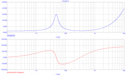
Nice plots. One of the things that's interesting about such overlapped SOA excursion plots is that the composite boundary turns out to be a straight line. This approach makes recognition of the fact that, for a fixed resistive series element (like voice coil R), those load impedances that have a significant phase angle also must have a higher impedance magnitude. In other words, if you are simulating into a woofer with 2 ohms Re, it would be pessimistic to assume an impedance magnitude of 2 ohms with a phase angle of 45 degrees.
I think this sort of thing was explained pretty well by Keith Howard in his Stereophile article awhile back.
Cheers,
Bob
what are you referring to.AndrewT say's, that isn't a problem; but after a look to the discussion here one must see different - so I think.
I cannot see what the questions you asked in that thread have anything to do with the discussion in this thread.
Please explain why you think these threads are related.
One of the things that's interesting about such overlapped SOA excursion plots is that the composite boundary turns out to be a straight line. ...
In other words, if you are simulating into a woofer with 2 ohms Re, it would be pessimistic to assume an impedance magnitude of 2 ohms with a phase angle of 45 degrees.
Hi Bob,
of course, for a resistive load we get a straight line.
Regarding 2 ohms Re, yes, it is a 'pesismistic' value, but in case of multiway speakers with 2 woofer drivers connected in parallel, you may get quite difficult load, depending on woofers used.
Regards,
Et al, here's my contribution: http://powerelectronics.com/mag/Ely January 2004 PET.pdf.
Hi Michael,
thanks for the interesting link.
Regards,
Hi Pavel,
Keeping that 25 mV under real-world junction temperature swings is not that easy.
Bob
if it s just "not that easy", then you are luckier than me...
quiescent current is purely devices dependant, from the
vbe circuit, whatever it is, diodes or vbe multiplier transistors,
then the drivers and to finish, the power devices...
in all this chain, no negative feedback that can be used to
correct the damn thing.....
this is the part of the amp where almost nothing has
changed since the arrival of the BJTS...
Hi Bob,
of course, for a resistive load we get a straight line.
Regarding 2 ohms Re, yes, it is a 'pesismistic' value, but in case of multiway speakers with 2 woofer drivers connected in parallel, you may get quite difficult load, depending on woofers used.
Regards,
Hi Pavel,
Let me see if I can explain my point better. If you have a reactive load with a minimum resistive impedance in series, as Re of a woofer is in series with a reactive tank circuit, in order to get a phase angle of the resulting net impedance you have to add reactive impedance in series with that initial resistance. If you add j2 ohms to 2 ohms, you get an impedance with a magnitude of 2.8 ohms and a phase angle of 45 degrees. If you add j100 ohms in series with 2 ohms, you get a phase angle of nearly 90 degrees, but the magnitude of that impedance is over 100 ohms.
The straight line that is formed by the overlapped boundaries of all of the reactive impedance loci is the equivalent of a resistive load line that extends from 0V to twice the rail voltage, as is easily seen from your nice set of overlapped plots. The resistance value of this resistive load line is twice the resistance of Re, where Re is the real resistance effectively in series with the reactive component of the load impedance.
If you have a loudspeaker whose impedance dips to 2 ohms, then what I am calling Re is 2 ohms. Clearly, the phase angle is zero at the point of the minima, so this is the real component. The maximum V-T boundary of the overlapped loci of all possible reactive combinations for this loudspeaker will form a resistive "load line" with a slope of 4 ohms, and which extends to 100V if the rails are +/- 50V. This observation is extremely useful because all we care about is the VI excursion boundary for all impedance combinations as a function of frequency, regardless of how those impedances originated (e.g., woofer resonance, crossover impedance peaks and dips, etc.).
This is a very convenient observation, but it is NOT the same as saying that the amplifier need only support a 4 ohm load, since a 4 ohm load only extends to Vrail, NOT 2 * Vrail. This is a very important distinction.
Cheers,
Bob
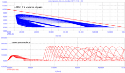
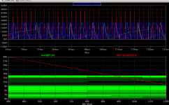
Here is an example of the line Bob wrote about. Is it correct that there are 4 pairs of devices on +-80V and that the same load circuit with Re = 2 ohms was used to generate these ellipses? This does not take into account that there is still some voltage drop (15V??) when the amplifier clips so this is why the ellipses do not quite reach the red line.
However, if more than one frequency is present then the load line can go outside even this line. The time spent outside (and even near it at high Vce:s) is short though for sensible signals.
However, if more than one frequency is present then the load line can go outside even this line. The time spent outside (and even near it at high Vce:s) is short though for sensible signals.
Attachments
Last edited:
The straight line that is formed by the overlapped boundaries of all of the reactive impedance loci is the equivalent of a resistive load line that extends from 0V to twice the rail voltage, as is easily seen from your nice set of overlapped plots. The resistance value of this resistive load line is twice the resistance of Re, where Re is the real resistance effectively in series with the reactive component of the load impedance.
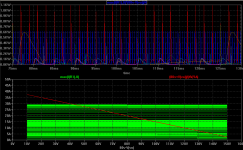
This applies only to sinus. For square signal is much worse.
Here's +-70V and +-40V fast rise time square waves at a couple of different frequencies with PMA's load circuit 4 pairs of devices on +-80V. The upper diagram shows dissipation. In the lower diagram the red line is the one Bob wrote about while the green mess is the load lines.
The rise time of the square wave matters. If it is slow then it won't be nearly this bad. Countering the inductive rise in impedance toward high frequencies with a zobel also makes it much better. Also, one has to wonder whether or not a full power fast rise time square wave really is a valid signal.
These large dissipation peaks that can be seen are very short. It's really more of a problem of protection circuit design than transistor SOA.
4 pairs of devices on +-80V. The upper diagram shows dissipation. In the lower diagram the red line is the one Bob wrote about while the green mess is the load lines.The rise time of the square wave matters. If it is slow then it won't be nearly this bad. Countering the inductive rise in impedance toward high frequencies with a zobel also makes it much better. Also, one has to wonder whether or not a full power fast rise time square wave really is a valid signal.
These large dissipation peaks that can be seen are very short. It's really more of a problem of protection circuit design than transistor SOA.
Attachments
These large dissipation peaks that can be seen are very short. It's really more of a problem of protection circuit design than transistor SOA.
And the 1-millisecond SOA can be many times the DC capability. At 100us, the FB SOA of a bipolar transistor is darn near square. A response time for the protection circuit on that order of magnitude is quite sufficient. You usually end up needing to slow it down to allow those 100us peaks to exceed the "low frequency" limit.
Hi Bob,
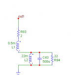
my parallel woofer model under simulation was as attached, which is IMO not so far from reality.
Regards,
Hi Pavel,
I agree, this is a quite reasonable woofer model. It represents what would be agressively rated as a 4 ohm speaker. It would represent an "honestly" rated speaker, by conventional standards, of a little less than 3 ohms.
Cheers,
Bob
This applies only to sinus. For square signal is much worse.
Yes, it is possible to concoct drive signals into reactive loads that create extraordinarily high current; not just square waves, but arbitrary pulse functions. Take a look at my IIM paper on my web site at Cordell Audio: Home Page. Such concocted waveforms can create large V-I excursions that will violate SOA boundaries, but such excursions tend to be very brief. The SOA for a very brief interval for a transistor is quite high.
Cheers,
Bob
SOA is all about peak junction temperature
Here are some thought about what governs the SOA boundary and how SOA must be de-rated at case temperatures above 25C.
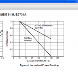
SOA is all about peak junction temperature. Consider an MJL21193. It is rated at 200W with a maximum junction temperature of 150C. This means the junction can rise from a 25C case temperature by 125C, implying a junction-to-case thermal resistance of 0.625 C/W. This is an average power dissipation calculation, not an SOA calculation. Heat is the enemy of reliability. The 150C junction temperature comes from a long term reliability target. Such a target might be 1% failures in ten years if the device is operated continuously at a junction temperature of 150C. This could happen in a continuous-duty DC voltage regulator, for example.
SOA in the context that we are discussing has more to do with destruction as opposed to long term reliability. It has to do with the peak die temperature that will cause the device to destruct (resulting from a reactive load V-I excursion, for example). This peak destruct junction temperature is necessarily higher than the maximum rated junction temperature (otherwise there would be no long-term reliability margin). And yet the published DC SOA curve follows the long-term power dissipation curve (apart from the secondary breakdown region). When they say DC, they really mean DC for like ten years. And yet this is not the destruct point. So we know that we have some margin built in with regard to concerns about device destruction. This is a good thing. This is part of the reason why the SOA is often shown as being larger for short periods of exposure like 100 ms; there are package and die temperature time constants that delay the time when the junction temperature will reach the rated junction temperature of 150C.
Some manufacturers leave it at that as far as publishing the SOA boundary; they define the SOA boundary as the point at which the peak die temperature reaches 150C. There is thus still some margin built into the plot because the 150C number is a long term reliability limit. IRF specs the SOA of their HEXFETs this way, for example. Actual destruction for them occurs at a peak junction temperature of about 300C. So there is still some margin in the curves, and this is a good thing. Bear in mind that MOSFETs will not necessarily behave in the same way as BJTs in regard to destruct point.
The second breakdown region that begins at higher voltages (70V for the MJL21193) effectively represents a reduced allowed maximum peak junction temperature than 150C. You will see that the SOA boundary for the MJL21193 is a constant 200+ watts up to 70V. By the time you reach 100V, allowable power dissipation has dropped to about 180W, analogous to a lower allowed junction temperature. At 250V, allowed DC power dissipation is down to about 100W.
Proper de-rating of SOA is important in a real application. In the non-second-breakdown region this is straightforward. It is no different than power dissipation de-rating. A 21193 operating at a case temperature of 70C will only allow for a junction temperature rise of 80C with a thermal resistance of 0.625C/W, implying a de-rated power dissipation of 128W. This corresponds to a linear de-rating factor of 64%.
De-rating of SOA in the second breakdown region is a bit less clear. If you go with the reduced allowed peak junction temperature theory, at 250V you have 100W dissipation at a case temperature of 25C and a thermal resistance of 0.625C/W. This corresponds to an allowed junction rise of 62.5C and a peak junction temperature of 25 + 62.5 = 87.5C. If the case temperature is 70C, this allows for only a 17.5C rise to junction at 0.625 C/W, corresponding to only 28W. By this theory, the numbers get ugly fast. This theory may result in an unintended conservative result for de-rating.
A less conservative approach to de-rating in the second breakdown region simply uses the same linear de-rating factor found for dissipation, namely 64% in this example, leading to allowable power dissipation of 64W at 250V.
Which approach to second-breakdown de-rating do you guys think is appropriate?
None of this long-winded post is meant to imply that you should not adhere to the manufacturer’s SOA curves, but rather to provide some understanding and to show that there is a bit of safety margin under some conditions. The amount of safety margin in the important second-breakdown region as a result of the long-term reliability vs. destruct threshold junction tempertures is less clear.
Cheers,
Bob
Here are some thought about what governs the SOA boundary and how SOA must be de-rated at case temperatures above 25C.
SOA is all about peak junction temperature. Consider an MJL21193. It is rated at 200W with a maximum junction temperature of 150C. This means the junction can rise from a 25C case temperature by 125C, implying a junction-to-case thermal resistance of 0.625 C/W. This is an average power dissipation calculation, not an SOA calculation. Heat is the enemy of reliability. The 150C junction temperature comes from a long term reliability target. Such a target might be 1% failures in ten years if the device is operated continuously at a junction temperature of 150C. This could happen in a continuous-duty DC voltage regulator, for example.
SOA in the context that we are discussing has more to do with destruction as opposed to long term reliability. It has to do with the peak die temperature that will cause the device to destruct (resulting from a reactive load V-I excursion, for example). This peak destruct junction temperature is necessarily higher than the maximum rated junction temperature (otherwise there would be no long-term reliability margin). And yet the published DC SOA curve follows the long-term power dissipation curve (apart from the secondary breakdown region). When they say DC, they really mean DC for like ten years. And yet this is not the destruct point. So we know that we have some margin built in with regard to concerns about device destruction. This is a good thing. This is part of the reason why the SOA is often shown as being larger for short periods of exposure like 100 ms; there are package and die temperature time constants that delay the time when the junction temperature will reach the rated junction temperature of 150C.
Some manufacturers leave it at that as far as publishing the SOA boundary; they define the SOA boundary as the point at which the peak die temperature reaches 150C. There is thus still some margin built into the plot because the 150C number is a long term reliability limit. IRF specs the SOA of their HEXFETs this way, for example. Actual destruction for them occurs at a peak junction temperature of about 300C. So there is still some margin in the curves, and this is a good thing. Bear in mind that MOSFETs will not necessarily behave in the same way as BJTs in regard to destruct point.
The second breakdown region that begins at higher voltages (70V for the MJL21193) effectively represents a reduced allowed maximum peak junction temperature than 150C. You will see that the SOA boundary for the MJL21193 is a constant 200+ watts up to 70V. By the time you reach 100V, allowable power dissipation has dropped to about 180W, analogous to a lower allowed junction temperature. At 250V, allowed DC power dissipation is down to about 100W.
Proper de-rating of SOA is important in a real application. In the non-second-breakdown region this is straightforward. It is no different than power dissipation de-rating. A 21193 operating at a case temperature of 70C will only allow for a junction temperature rise of 80C with a thermal resistance of 0.625C/W, implying a de-rated power dissipation of 128W. This corresponds to a linear de-rating factor of 64%.
De-rating of SOA in the second breakdown region is a bit less clear. If you go with the reduced allowed peak junction temperature theory, at 250V you have 100W dissipation at a case temperature of 25C and a thermal resistance of 0.625C/W. This corresponds to an allowed junction rise of 62.5C and a peak junction temperature of 25 + 62.5 = 87.5C. If the case temperature is 70C, this allows for only a 17.5C rise to junction at 0.625 C/W, corresponding to only 28W. By this theory, the numbers get ugly fast. This theory may result in an unintended conservative result for de-rating.
A less conservative approach to de-rating in the second breakdown region simply uses the same linear de-rating factor found for dissipation, namely 64% in this example, leading to allowable power dissipation of 64W at 250V.
Which approach to second-breakdown de-rating do you guys think is appropriate?
None of this long-winded post is meant to imply that you should not adhere to the manufacturer’s SOA curves, but rather to provide some understanding and to show that there is a bit of safety margin under some conditions. The amount of safety margin in the important second-breakdown region as a result of the long-term reliability vs. destruct threshold junction tempertures is less clear.
Cheers,
Bob
Here are some thought about what governs the SOA boundary and how SOA must be de-rated at case temperatures above 25C.[snip]Cheers,
Bob
Great post Bob, thanks!
jd
Which approach to second-breakdown de-rating do you guys think is appropriate?
Bob
The linear derating factor. If you look at Moto/On's s/b ratings, especially for switching transistors, they publish two derating curves. One for thermal, and another for s/b. The s/b derating curve is actually even less conservative - it does not derate all the way to zero at 200C.
Attachments
The linear derating factor. If you look at Moto/On's s/b ratings, especially for switching transistors, they publish two derating curves. One for thermal, and another for s/b. The s/b derating curve is actually even less conservative - it does not derate all the way to zero at 200C.
Thank you! This is a very nice find. The result is very encouraging.
Thanks,
Bob
I agree, great post Bob! Thanks.
I'm quite interested in the safety margins myself so have done some research on the issue. As for what happens at different temperatures the 150 degree (or 175 for some parts) limit is, from what I can find, a limit that comes from the plastic material itself. Temperature should be kept below this so that the package does not degrade. Keeping average junction temperature below 150 degrees should even be enough out of concern for the plastic.
Just as you say, the destruction temperature is much higher than this value. For example, the "SPiKe" protection in the LM3886 is set to activate at a junction temperature of 250 degrees C and this part uses BJT outputs, so it's not just MOSFET:s that survive high temperatures. (SPiKe AN)
John Larkin on sci.electronics.design did some tests with power MOSFET:s similar to those you have made and he came to the conclusion that failure happens at around 350 degrees C for those. At 300 degrees, they wouldn't turn off however so in a typical amplifier circuit they would be doomed already by then. (Try this link to Google Groups.)
I've come to similar conclusions myself too. After torturing a couple of lateral MOSFET:s at 100 degrees case temperature and somewhat more than 150% of rated room temperature dissipation for a couple of minutes I gave up. They still worked.
As for second breakdown there seems to be two different effects that get grouped into this. One is that as collector voltage increases the current will crowd towards the emitter finger edges, effectively increasing the thermal resistance. (OnSemi AN) This is essentially a thermal limitation; the temperature at these hottest spots must be kept low enough. If it gets high enough the transistor will, just as a MOSFET, be unable to turn off at these spots.
The other one is the often described hotspotting. If the positive thermal feedback becomes too great somewhere hotspots will form and the transistor will be doomed. Vertical MOSFET:s may suffer from this too, not only BJT:s, like those trench parts linked to earlier in this thread. However, this behaviour does not necessarily degrade with temperature. Above a certain Ic at a certain Vce, the transistor may get destroyed, regardless of if it is cold or hot.
In the following datasheets there are some interesting graphs. Page 3 of the LM12 datasheet and page 9 of the LM3886 datasheet contain graphs showing thermal resistance VS Vce and even transient thermal plots at different collector voltages. Here it can be seen how the thermal resistance increases with collector voltage and also the the degradation towards higher voltages gets less severe the hotter the transistor gets.
Many datasheets show that the second breakdown need not be derated as much as the power dissipation rating. This fits well with the 100ms pulse thermal resistance plot for different temperatures shown in the LM3886 datasheet.
A Sanken transistor handbook I saw once said in passing that the second breakdown ratings need not be derated as much because the destruction temperature is in the range 250-350 degrees. They suggested that the second breakdown curves be derated as if they would result in a junction temperature of 250 degrees. This would mean a derating to ~65% at 100 degrees case temperature, something that fits well with many datasheets I've seen which have different derating factors for S/B and thermal limits. The OnSemi appnote is even less restrictive: 75%.
It is sometimes unclear how much margin there is in the SOA plots of BJT:s however. MOSFET:s almost always have calculated SOA plots, both DC and pulse, based on 150 or 175 degree peak temperature so in that case there are large margins as long as they are thermally stable. But for BJT:s, at least in the past, the plots could be based on destructive testing with a little margin added.
In some cases, such as for the 2SA1943 the SOA plot and transient thermal resistance can be compared. Here it seems like the thermal limits in the SOA plot, both DC and pulse, are based on a ~150 degree peak junction temperature which would be nice and conservative.
How the second breakdown limits were arrived at can't be determined this way though. If they too are based on a peak 150 degree temperature at the hottest spot they would be quite conservative. If they are based on destruction or 250 degree peak temperature I wouldn't want to push it on the other hand. It is probably safest to assume this is the case, build a circuit to measure (transient) thermal impedance by junction drop at a couple of different voltages, or test the margins by blowing up a couple of them under controlled conditions. The last option might be the most fun, but maybe a bit expensive.
Another way of coming to conclusions of how much is needed is to look at what's done in commercial equipment of good quality and reputation. Some manufacturers have 5 year warranties for example, and in that case it's much cheaper to add a couple of output devices than risk warranty returns. Still, these products often have less output device SOA than what many frequents of this site consider an absolute minimum for reliability. Still these amplifiers hold up in club applications where they are used night in and night out.
Designing for an absolute worst case average junction temperature of 150 degrees (at impedance dips) often seem to give similar results in the needed amount of output devices as what commercial manufacturers with good reputation use. Actually, that ends up with, for 150W transistors on a 60 deg C heatsink, about 150W of output per pair at the lowest rated impedance (dips to half of that are allowed) if rail loss is negligible. That's about 75W per pair at 8 ohms if 4 ohm speaker loads are to be allowed. Hmm... I belive I saw that number just some minutes ago somewhere else...
If I did the calculations correctly, the absolute worst case average output stage dissipation (if idle is reasonably low) for any input signal can be determined as:
Total output stage dissipation = Vcc ^ 2 / (4 * Re)
where Vcc = rail voltage of a single rail (e.g. 40V for +-40V rails) and Re = the impedance at the lowest impedance dip. This is the same dissipation as for a half rail voltage square wave into a resistive load with the same resistance as the impedance at the dip. This dissipation is a little bit, but not much, higher than the worst case sinewave into a resistive load of Re. It is about 10-20% (I don't remember the exact number) lower for a worst-case sine wave than for the square wave. Music will be even lower than the sine, so there is even more conservativeness than those tens of percent built into this.
Oops, this became a long post. I hope it will be useful
I'm quite interested in the safety margins myself so have done some research on the issue. As for what happens at different temperatures the 150 degree (or 175 for some parts) limit is, from what I can find, a limit that comes from the plastic material itself. Temperature should be kept below this so that the package does not degrade. Keeping average junction temperature below 150 degrees should even be enough out of concern for the plastic.
Just as you say, the destruction temperature is much higher than this value. For example, the "SPiKe" protection in the LM3886 is set to activate at a junction temperature of 250 degrees C and this part uses BJT outputs, so it's not just MOSFET:s that survive high temperatures. (SPiKe AN)
John Larkin on sci.electronics.design did some tests with power MOSFET:s similar to those you have made and he came to the conclusion that failure happens at around 350 degrees C for those. At 300 degrees, they wouldn't turn off however so in a typical amplifier circuit they would be doomed already by then. (Try this link to Google Groups.)
I've come to similar conclusions myself too. After torturing a couple of lateral MOSFET:s at 100 degrees case temperature and somewhat more than 150% of rated room temperature dissipation for a couple of minutes I gave up. They still worked.
As for second breakdown there seems to be two different effects that get grouped into this. One is that as collector voltage increases the current will crowd towards the emitter finger edges, effectively increasing the thermal resistance. (OnSemi AN) This is essentially a thermal limitation; the temperature at these hottest spots must be kept low enough. If it gets high enough the transistor will, just as a MOSFET, be unable to turn off at these spots.
The other one is the often described hotspotting. If the positive thermal feedback becomes too great somewhere hotspots will form and the transistor will be doomed. Vertical MOSFET:s may suffer from this too, not only BJT:s, like those trench parts linked to earlier in this thread. However, this behaviour does not necessarily degrade with temperature. Above a certain Ic at a certain Vce, the transistor may get destroyed, regardless of if it is cold or hot.
In the following datasheets there are some interesting graphs. Page 3 of the LM12 datasheet and page 9 of the LM3886 datasheet contain graphs showing thermal resistance VS Vce and even transient thermal plots at different collector voltages. Here it can be seen how the thermal resistance increases with collector voltage and also the the degradation towards higher voltages gets less severe the hotter the transistor gets.
Many datasheets show that the second breakdown need not be derated as much as the power dissipation rating. This fits well with the 100ms pulse thermal resistance plot for different temperatures shown in the LM3886 datasheet.
A Sanken transistor handbook I saw once said in passing that the second breakdown ratings need not be derated as much because the destruction temperature is in the range 250-350 degrees. They suggested that the second breakdown curves be derated as if they would result in a junction temperature of 250 degrees. This would mean a derating to ~65% at 100 degrees case temperature, something that fits well with many datasheets I've seen which have different derating factors for S/B and thermal limits. The OnSemi appnote is even less restrictive: 75%.
It is sometimes unclear how much margin there is in the SOA plots of BJT:s however. MOSFET:s almost always have calculated SOA plots, both DC and pulse, based on 150 or 175 degree peak temperature so in that case there are large margins as long as they are thermally stable. But for BJT:s, at least in the past, the plots could be based on destructive testing with a little margin added.
In some cases, such as for the 2SA1943 the SOA plot and transient thermal resistance can be compared. Here it seems like the thermal limits in the SOA plot, both DC and pulse, are based on a ~150 degree peak junction temperature which would be nice and conservative.
How the second breakdown limits were arrived at can't be determined this way though. If they too are based on a peak 150 degree temperature at the hottest spot they would be quite conservative. If they are based on destruction or 250 degree peak temperature I wouldn't want to push it on the other hand. It is probably safest to assume this is the case, build a circuit to measure (transient) thermal impedance by junction drop at a couple of different voltages, or test the margins by blowing up a couple of them under controlled conditions. The last option might be the most fun, but maybe a bit expensive.
Another way of coming to conclusions of how much is needed is to look at what's done in commercial equipment of good quality and reputation. Some manufacturers have 5 year warranties for example, and in that case it's much cheaper to add a couple of output devices than risk warranty returns. Still, these products often have less output device SOA than what many frequents of this site consider an absolute minimum for reliability. Still these amplifiers hold up in club applications where they are used night in and night out.
Designing for an absolute worst case average junction temperature of 150 degrees (at impedance dips) often seem to give similar results in the needed amount of output devices as what commercial manufacturers with good reputation use. Actually, that ends up with, for 150W transistors on a 60 deg C heatsink, about 150W of output per pair at the lowest rated impedance (dips to half of that are allowed) if rail loss is negligible. That's about 75W per pair at 8 ohms if 4 ohm speaker loads are to be allowed.
Hmm... I belive I saw that number just some minutes ago somewhere else... If I did the calculations correctly, the absolute worst case average output stage dissipation (if idle is reasonably low) for any input signal can be determined as:
Total output stage dissipation = Vcc ^ 2 / (4 * Re)
where Vcc = rail voltage of a single rail (e.g. 40V for +-40V rails) and Re = the impedance at the lowest impedance dip. This is the same dissipation as for a half rail voltage square wave into a resistive load with the same resistance as the impedance at the dip. This dissipation is a little bit, but not much, higher than the worst case sinewave into a resistive load of Re. It is about 10-20% (I don't remember the exact number) lower for a worst-case sine wave than for the square wave. Music will be even lower than the sine, so there is even more conservativeness than those tens of percent built into this.
Oops, this became a long post. I hope it will be useful
Last edited:
- Status
- This old topic is closed. If you want to reopen this topic, contact a moderator using the "Report Post" button.
- Home
- Amplifiers
- Solid State
- Output transistor safe operating area