I tried with 330pF shunt compensation, but the amp is totaly unstable with that value (without Jan's 50p+10R on driver's bases). Optimal is 150-220pF C3, C5. However there was a slow motorboating oscillation heard. I removed it with help of C12, C24 capacitors. Now I can rise the input bias to 4mA without issues. But the scope still shows the oscillation left, perhaps lowering the value of C12, C24 might help.
mooving C12 from emitter to kollektor of Q16
mov c24 to kollektor of Q17
I have already done that but before posting anything about this please post photographs of your hardware and the power supply set up as used in the foregoing tests.
Sorry for late reply. But I don't think it's necessary, as I'm not going to use these now flawed PCBs.
Yes, I wrote about it in post 656.Have you ever considered why this is?
You might think of the value of the emitter resistor value in terms of the length of studs on winter sports foot-wear. I suggest you read what Bob Cordell had to say in post 293 on page 30.
Bob said he hasn't used such a low value emitter resistors, but Roender has in his FC-100 amp. So, it's practicaly proved lower value emitter resistors are beneficial in terms of XOD, the only disadvantage is Pd and need of tight match. However I don't mind 0R22 to be used in the schematic, it should be almost the same in terms of XOD I suppose and I doubt it can affect the stability much.
Andriy, don't give up on the present PCB just yet because there is one sure way to stop oscillations that you can use.
Also, in simulations using the same component values as your PCB amp you can see any differences in the squarewave tests, and then you adjust you simulation to make it do what your PCB amp does. Then you can use simulations to probe PM and GM with different modifications that are hard to do with bench testing.
As I wrote to Michael, I'm not going to use these boards, than don't need to bother to make it to work.
I can't do this alone. I trust you to perform complicated sim tests.
Attachments
![20180612_224835[1].jpg](/community/data/attachments/634/634508-6fa6bc9f1db7e920f8873416ad6b4905.jpg)
![20180612_224501[1].jpg](/community/data/attachments/634/634525-e52129ac5c731909f0bfb3d026df85a9.jpg)
As I wrote to Michael, I'm not going to use these boards, than don't need to bother to make it to work.
I can't do this alone. I trust you to perform complicated sim tests.
I don't know if there is salvation for your boards but they may still serve a useful purpose to see if the compensation method suggested by R Dijk has any impact.
While you have concerns about board layout - apparently over a wide area looking at your prototype I have a memory of seeing something like this illustrated by Nelson Pass in his A40 amplifier that could only be described as a lash up albeit this was a prototype for a cleaned up version.
This amplifier uses the same compensation as suggested above. The simulation I did awaiting your reply also uses this method.
While you may not be a Nelson Pass you have nothing to lose by trying what he did.
The problem you have with the present of form of lag compensation is that it is defeated by the changes in phase in the output stage which it cannot control due to the decrease in your supply rails.
That does not matter with the scheme suggested since if there is any current flow through the Vas stage a sample of that will get to the inverting input terminal unaffected by the changes in phase at the output.
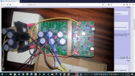
It is not clear still if you are using a safety bulb or a variac to reduce the supply voltages but you can run the whole amplifier for a test with 5W 100R serial resistors between the supply and the board - just using the larger transformer and its' supply.
I have run a Tian test which indicates good stability margins under these conditions.
I have used a single 470 pF capacitor - you could reduce this to 220pF and fit another 220 pf on the opposite side of the circuit.
Attachments
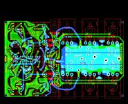
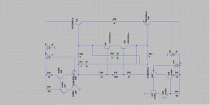
I checked this compensation suggested by R Dijk but bulb tester was shine at full power. I didn't work. I have what to loose, the components might not survive in the worst case. My current supply rails are lower than in the schematic. It can only be raised by transformer mod, which I can't do by now. Inverting input is cut off. The PCB works in SE config. I'm using a bulb, it's more informative in what's going on. I don't have such resistor. Do you mean transformer primary as resistor? Previous test showed the amp don't want to work with 330pF compensation. With higher value should be the same. Your sim has different output stage than I'm using now. My current pcb layout.
Attachments
Last edited:
Part of the set up process involves setting trimmer for the appropriate level of output stage Iq by measuring the voltage drop across the 5 W resistors shown in my simulation between the supply rails and the circuit itself. The current draw can be calculated from the voltage drop across these resistors from Ohms law. For example a 10 volt drop equates to 100 mA.
If the circuit is stable you should be able to reduce the current drawn from the supply to a level that would be safer to remove the resistors and apply the rails directly.
The circuit board outline shows where the trimmer is. In your actual hardware I see a capacitor which is smaller than the other trimmers so it has to be absent.
If you have replaced this with a resistor for a current drawn by the output stage of roughly 500 mA as indicated by some simulations. That could explain a few things - so you need to see this is not the cause of your problems.
Increasing the trimmer resistance will reduce the Iq and if you have a resistor instead of a trimmer you can even cut the end of one lead to reduce Iq.
Keep a finger on the body of the 5 W resistor and the other on the power switch. If you feel this rapidly getting hot as in a surge turn the equipment off immediately.
Attachments
Obviously, Ft of the BJT transistor isn't the same as switching speed, which is the sum of Delay time (td), Rise time (tr), Fall time (tf), Storage time (ts) Limiting factors are parasitic capacitances, inductance and operating conditions. So, smaller transistors should be faster than bigger ones.It seems that drivers are usually slower than pre-drivers (is it due to die size?).
FETs are faster and perhaps can be advantageous in this regard.
Agreed. Here's perhaps a better way to speed-up the CFP driver's turn-off. Reduce the value of the driver's base-emitter resistors.
With 25 ohms they turn off as fast as my previous base-base capacitor method. And there is no rail coupling issues with lower base-emitter resistors. But the pre-driver now dissipates 4 times the power.
To keep the simplicity, I suppose 1W Pd with heatsink should not be a problem.
Last edited:
I checked this compensation suggested by R Dijk but bulb tester was shine at full power. I didn't work. I have what to loose, the components might not survive in the worst case. My current supply rails are lower than in the schematic. It can only be raised by transformer mod, which I can't do by now. Inverting input is cut off. The PCB works in SE config. I'm using a bulb, it's more informative in what's going on. I don't have such resistor. Do you mean transformer primary as resistor? Previous test showed the amp don't want to work with 330pF compensation. With higher value should be the same. Your sim has different output stage than I'm using now. My current pcb layout.
Ya gotta start somwhere. if ypu look close at Hegglund's setup it is a werry good start.
Attachments
Sorry, but I don't understand what do you mean. I started with real built a long time ago. Is this your schematic modification?Ya gotta start somwhere. if ypu look close at Hegglund's setup it is a werry good start.
Sorry, but I don't understand what do you mean. I started with real built a long time ago. Is this your schematic modification?
Sorry abt that.
Yes, with the load as is.... My quick test on earlier values and then your testload, eksperiments gave me thise values. Havent tested with no load!
First time i saw this circ was i loooooooooooong time ago publiched here by Kenatoken.
And some nice treads with some good discussions way back.
")
And sorry for my lang=0, typing is defenetlyy not my side.
The trimmer is behind the heatsink 10K, as I wrote before. 500R was too low. With 10K trimmer setting and 4mA input bias I have 2.5mV on output emitter resistors
If you are still using the safety bulb test method try measuring some base to emitter voltages which should be roughly 0.6 volts to see where the shortfall in conduction is - quite likely it will be wide spread.
Ya gotta start somwhere. if ypu look close at Hegglund's setup it is a werry good start.
Nice simulation - an ideal model in my view.
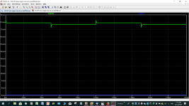
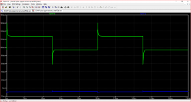
Looking into this - two plots attached show 1. square wave in test set up minus parallel capacitor to the load first in test set up and 2. at high power.
Others should note the switching time for Q19 as compared with Q21 which has more to do with the amounts of emitter current than comparisons of transistor speeds.
Attachments
maybee thise or a pair each side ?
.MODEL KSA1220A_k PNP (IS=4.7863E-13 BF=289.3 NF=1.0 BR=9.76 NR=1.006 ISE=5.2481E-12 NE=2 ISC=2.4909E-11 NC=1.5 VAF=98.5 VAR=6.7 IKF=2.7061 IKR=0.0759 RB=2.26 RBM=0.2308 IRB=0.001 RE=0.1908 RC=1.1748 QCO=0.02 RCO=3.9811 VO=11.078 GAMMA=5.01187E-8 CJE=3.4786E-10 VJE=0.9575 MJE=0.4694 FC=0.5 CJC=1.1224E-10 VJC=0.5761 MJC=0.4365 XCJC=0.4955 XTB=1.7978 EG=1.2255 XTI=3.0 Tf=970p Vceo=160 Icrating=1.2A mfg=Fairchild)
.MODEL KSC2690A_k NPN ( IS=1.7783E-13 BF=132.5 NF=1.0 BR=8.495 NR=1.005 ISE=1.9953E-13 NE=1.5 ISC=1.5849E-9 NC=1.98 VAF=580.75 VAR=18.15 IKF=4.0271 IKR=0.0120 RB=2.98 RBM=0.001 IRB=0.6396 RE=0.0909 RC=1.4705 QCO=0 RCO=0 VO=6.587 GAMMA=2.8216E-7 CJE=4.0082E-10 VJE=0.6696 MJE=0.3296 FC=0.5 CJC=6.0404E-11 VJC=0.5 MJC=0.4266 XCJC=0.4955 XTB=1.2590 EG=1.2277 XTI=3.0 Tf=830p Vceo=160 Icrating=1.2A mfg=Fairchild)
C10 and C11 is doing nothing but fighting C4 and C6 witch is decopling the caskode, i would remove C10 and C11 or find a better place. decupling with capasitors of different types in series ? It would bee nice to see one good argument for doing this???
I am still wondering if this circ is temperature stable tracking ? Is the input stage giving output current tracking temperature varation in vas stage in som way ? Current sorce tracking near vas transistors maybee ? Anny simmulated temperature sveep? Calculated requiered cooling fin ? Difference with different types of insulating pads... etc etc
BTW here is a idea:
setting the vas transistors up as darlington wil give the possibillity to increase open loop gain by near 2 . BUT AL LOT HARDER TO TEMP TRACK
..... (BUT GET WHAT YOU HAVE STABLE FIRST !)
EXAMPLE attached.
Attachments
If you are still using the safety bulb test method try measuring some base to emitter voltages which should be roughly 0.6 volts to see where the shortfall in conduction is - quite likely it will be wide spread.
Input bjts have 0.560-0.567V, small VAS bjts - 0.62V\0.627V, bigger VAS bjts - 0.65V.
With 3mA input bias the differens between PSUs 10V, with 4mA bias front end voltage sags to the same voltage as at output.
On 5V zeners should there be 5V drop from initial voltage or 5V on output of zeners? I'm using tl431 instead of zeners.
Before I tried to remove them but the amp didn't work. Forgot to report about it.C10 and C11 is doing nothing but fighting C4 and C6 witch is decopling the caskode, i would remove C10 and C11 or find a better place. decupling with capasitors of different types in series ? It would bee nice to see one good argument for doing this???
I am still wondering if this circ is temperature stable tracking ? Is the input stage giving output current tracking temperature varation in vas stage in som way ? Current sorce tracking near vas transistors maybee ? Anny simmulated temperature sveep? Calculated requiered cooling fin ? Difference with different types of insulating pads... etc etc
As I can see, output DC offset is quite stable from cold start to near hot conditions with tens of mV variations, considering my input transistors aren't thermally coupled. From simulation and theoretical point of view Ian could answer much further when he is back. Here is what he wrote about it before. CCS temp co of sim4 does compensate out the input transistor's temp co by about the right amount!
The OrgTempCo circuit displays the change in VAS currents when the temp is stepped from 27C to 47C. The temp co is about -0.14%/C. Negative means it is slightly over compensated.
The ZTempCo circuit shows the temperature coefficient can be zeroed out using a relatively high shunt resistor across each CCS. The THD is still about the same with the trimming R's.
But probably there isn't a need to trim the temp co out, since it is already compensated for ambient temperature variations that's assuming our models temperature coefficients are spot on.
Nice simulation - an ideal model in my view.
Looking into this - two plots attached show 1. square wave in test set up minus parallel capacitor to the load first in test set up and 2. at high power.
Others should note the switching time for Q19 as compared with Q21 which has more to do with the amounts of emitter current than comparisons of transistor speeds.
When im doing sim on your circ im getting som osc around sleving and iven som serius change in circ values did not help mee.... !!!!!!
So i did redraw it to make it easier to c what does what where and how. And insulating stages a bit easier for me. Maybee others too.
I never got happy with your input transistors in the voltage amplifier, nor for the driver.
So i used my sissors, cut and paste.
Here is a redraw of your input stage, WITH a medium, driver and output stage that sims fairly all right.
Now it is easyer to see the input stage as two mirrired single end.
Somthing like that you can use two j-fet and save making of current sorces !
Mentioning current sorces!!!! They are part of your circuit problems.
The collector emitter capasitor in the current sorces ( Q27 and Q28) is here making for an oscillator as it "delayes" the feedback.
Putting at least 1k in series with your current sorces will help a lot.... SoOOO i mooved them to the rails.
Btw here is a different output and voltage amp as mentioned, a shortcut with drivers directly in paralell, two by two utput is one possibillity.
Here is abt where i would start for a furter development, see attacment.
Attachments
Thanks for your time and efforts RDijk. However your schematic refuse to simulate without txt file. Could you please show how to use it with two j-fet (as input I guess) without current sorces? Is there a specific purpose of using 4 output transistors? More linear output, lower THD, low imp loads? As for me power wise, 3 is more than enough. Why have you used EF output stage? CFP is know to be more "musical". R12, R13 are really necessary in the circuit? Is it possible to make balanced or differential input with this topology? Let's wait for comments from technically advanced members.
Last edited:
put this in the schematic above as a spice directive, use .op button:
.MODEL KSC2690A_r NPN ( IS=1.7783E-13 BF=132.5 NF=1.0 BR=8.495 NR=1.005 ISE=1.9953E-13 NE=1.5 ISC=1.5849E-9 NC=1.98 VAF=580.75 VAR=18.15 IKF=4.0271 IKR=0.0120 RB=2.98 RBM=0.001 IRB=0.6396 RE=0.0909 RC=1.4705 QCO=0 RCO=0 VO=6.587 GAMMA=2.8216E-7 CJE=4.0082E-10 VJE=0.6696 MJE=0.3296 FC=0.5 CJC=6.0404E-11 VJC=0.5 MJC=0.4266 XCJC=0.4955 XTB=1.2590 EG=1.2277 XTI=3.0 Tf=830p Vceo=160 Icrating=1.2A mfg=Fairchild)
.MODEL KSA1220A_r PNP (IS=4.7863E-13 BF=289.3 NF=1.0 BR=9.76 NR=1.006 ISE=5.2481E-12 NE=2 ISC=2.4909E-11 NC=1.5 VAF=98.5 VAR=6.7 IKF=2.7061 IKR=0.0759 RB=2.26 RBM=0.2308 IRB=0.001 RE=0.1908 RC=1.1748 QCO=0.02 RCO=3.9811 VO=11.078 GAMMA=5.01187E-8 CJE=3.4786E-10 VJE=0.9575 MJE=0.4694 FC=0.5 CJC=1.1224E-10 VJC=0.5761 MJC=0.4365 XCJC=0.4955 XTB=1.7978 EG=1.2255 XTI=3.0 Tf=970p Vceo=160 Icrating=1.2A mfg=Fairchild)
I used the schematic just cause i had one output working fairly well.
The reason vas cause the output stage was for a class A that could handle fairly complex load ie having good power margins AND i had it in a LT .asc file ( easy copy and paste ).
BTW: You dont need Q29 and Q24, remove and jumb base emitter.
R12 R13, Yes they adjust the amount of common current rejection, ie sort of shot thru. And they increase termal compensation, as well as adding a base resistance to the drivers.
Too make your voltage amp work more syncron i added C12 in your design.
Ballanced ? and topologi wel depends, you make two mirrors and... but then what about topologi ?
This attached file with Jfet input dont need txt cause the models are in the file. Now the circuit input is near a PassLab F(somthing), but the rest of the circ is with transistors. Added diodes to protect vas stage.
The current generators are still here, for the ease of modif.
Attachments
Last edited:
Input bjts have 0.560-0.567V, small VAS bjts - 0.62V\0.627V, bigger VAS bjts - 0.65V.
With 3mA input bias the differens between PSUs 10V, with 4mA bias front end voltage sags to the same voltage as at output.
On 5V zeners should there be 5V drop from initial voltage or 5V on output of zeners? I'm using tl431 instead of zeners.
The TL431's contain an op.amp and have a bias network around them to work as shunt diodes.
It is possible in your set up mode a restriction of supply current is is having an effect on the biasing of the TL431's - reduced current flows through whatever resistor network you might have set up.
Your transistor measurements suggest these are in working order under current restricted conditions and that the output stage is hogging most of what is available.
If you don't have enough emitter current that means less base current and less Vbe.
Your measurements are close but not quite where they need to be.
Is it possible to make balanced or differential input with this topology?
Let's wait for comments from technically advanced members.
Here is an example of adding some components to make it BALANCED. I believe the open loop gain is lower, but can be increased by adding resistors/maybe jumpers source-source on the Jfets. This one must be symmetric.
ps in the troblesom file you need to remove the lib pointer also.
Attachments
- Status
- This old topic is closed. If you want to reopen this topic, contact a moderator using the "Report Post" button.
- Home
- Amplifiers
- Solid State
- One of the Top Solid-State CFA amp design