Mjona, Andriy,It appears the supply for the front end is not stiff enough - what are the voltage and VA ratings of the transformer for this section.
I had a thought about biasing. With "29V\37.5V on PSUs" the dropper resistors R10,R11 for the +/-15V zeners needs to be chosen so there is about 3-5mA through the zeners.
Andriy, do you have the right value for R10,R11 for 37.5V? If not, see below.
Sin5a has 17mA through R10,R11. With 37.5V for the input stage, less 5V for D3,D4 and 15V zeners there will be 17.5V across R10,R11. So R10,R11 need to be 1k each (1/2W will do).
Don't forget R10,R11 need changing again when going to the normal rail voltages.
Cheers
Edit, I just notice the post seconds ago before mine says 37.5V AC -- I assumed DC. That would be about 50V DC. So the dropper resistors work out to be 1.7k, the value already in sim5a.
Last edited:
Yes I have a right value of R10, R11, they are 1K 3W. I chose them before for balanced 8 input transistors load. If they were wrong value there is only 15V ssa bridge would sag, but not PSU output volatge. Excessive current consumption goes from Q16, Q17, perhaps due to oscillation, as I hear little noise from the speaker, positive input LED dims a bit when I touch the pcb or heatsink by hand.
I remember when I changed driver emitter resistors R22, R23 from 100 Ohms to 150 Ohms, Q16, Q17 became cooler as well as Q19, Q18
I remember when I changed driver emitter resistors R22, R23 from 100 Ohms to 150 Ohms, Q16, Q17 became cooler as well as Q19, Q18
Last edited:
Less complex CFP driver turn-off speed-up
With 25 ohms they turn off as fast as my previous base-base capacitor method. And there is no rail coupling issues with lower base-emitter resistors. But the pre-driver now dissipates 4 times the power. So I propose 4 existing pre-driver transistors in parallel with a 10R emitter sharing resistor for each pre-driver. Each driver dissipates the same power as the original circuit (~300mW).
A simulation (attached) shows 4 in parallel gives the best improvement for the number of extra parts. The plot below steps 1,2,3,4,5 pre-drivers, and Rbe is stepped 100R,50R,33R,25R,20R respectively.
Cheers
Agreed. Here's perhaps a better way to speed-up the CFP driver's turn-off. Reduce the value of the driver's base-emitter resistors.There is quite a lot of added complexity in the circuit. ...
With 25 ohms they turn off as fast as my previous base-base capacitor method. And there is no rail coupling issues with lower base-emitter resistors. But the pre-driver now dissipates 4 times the power. So I propose 4 existing pre-driver transistors in parallel with a 10R emitter sharing resistor for each pre-driver. Each driver dissipates the same power as the original circuit (~300mW).
A simulation (attached) shows 4 in parallel gives the best improvement for the number of extra parts. The plot below steps 1,2,3,4,5 pre-drivers, and Rbe is stepped 100R,50R,33R,25R,20R respectively.
Cheers
Attachments
![20180606_121741[1].jpg](/community/data/attachments/623/623874-fcf625f1b902be3910b25180597960dd.jpg)
Agreed. Here's perhaps a better way to speed-up the CFP driver's turn-off. Reduce the value of the driver's base-emitter resistors.
With 25 ohms they turn off as fast as my previous base-base capacitor method.
This will double the THD, if not consider shunt compensation.
What do you mean by "4 existing pre-driver transistors"? There is only 2 Q21, Q22 pre-driver transistors.
Mjona, Andriy,
I had a thought about biasing. With "29V\37.5V on PSUs" the dropper resistors R10,R11 for the +/-15V zeners needs to be chosen so there is about 3-5mA through the zeners.
Andriy, do you have the right value for R10,R11 for 37.5V? If not, see below.
Sin5a has 17mA through R10,R11. With 37.5V for the input stage, less 5V for D3,D4 and 15V zeners there will be 17.5V across R10,R11. So R10,R11 need to be 1k each (1/2W will do).
Don't forget R10,R11 need changing again when going to the normal rail voltages.
Cheers
Edit, I just notice the post seconds ago before mine says 37.5V AC -- I assumed DC. That would be about 50V DC. So the dropper resistors work out to be 1.7k, the value already in sim5a.
Just a general observation - the currents through R11 and R15 are practically equal by simulation.
The currents drawn from the supplies in this section are also equal but looking at the output stage there is a slight disparity due to the dc offset which has crept up somewhat through the process of development.
Changing R9 to 57.1R reduces this and the disparity, however if this setting is changed in either direction by 0.1R this causes significant changes in the dc output voltage and the potential of drift with temperature.
I would have thought the full voltage could have been applied to the input section.
I tried with 330pF shunt compensation, but the amp is totaly unstable with that value (without Jan's 50p+10R on driver's bases). Optimal is 150-220pF C3, C5. However there was a slow motorboating oscillation heard. I removed it with help of C12, C24 capacitors. Now I can rise the input bias to 4mA without issues. But the scope still shows the oscillation left, perhaps lowering the value of C12, C24 might help.
Attachments
Last edited:
4 pre-driver transistors are in parallel with a 10R emitter sharing resistor on each: 4xQ21 are 4x2SC3423 and 4xQ22 are 4x2SC1360.This will double the THD, if not consider shunt compensation.
What do you mean by "4 existing pre-driver transistors"? There is only 2 Q21, Q22 pre-driver transistors.
I did not draw 4 in parallel on the circuit. That may have confused things
 I used an area scaling parameter instead so I could simulate a variable number of transistors in parallel with one simulation.
 The extra base capacitance with 4 pre-driver (pairs) does not seem to affect the PM (approx 57deg).
The THD at 20kHz 15V with 4 pre-drvers reads 4.7ppm vs. 3.1ppm with one driver. Comp 220pF +10R.
The THD at 20kHz 15V with CFP base-base speed-up (50n+10R) and emitter decoupling (1R+68uF) reads 4.1ppm vs. 3.1ppm with no CFP speed-up.
If you wanted CFP speed-up, of the two options I'd take the more conventional paralleling of pre-drivers. A THD of 5ppm at 20kHz is excellent enough
.Cheers
I tried with 330pF shunt compensation, but the amp is totaly unstable with that value (without Jan's 50p+10R on driver's bases). Optimal is 150-220pF C3, C5. However there was a slow motorboating oscillation heard. I removed it with help of C12, C24 capacitors. Now I can rise the input bias to 4mA without issues. But the scope still shows the oscillation left, perhaps lowering the value of C12, C24 might help.
It is not clear if you have sorted the front end power supply - what voltage level are the rails at for this test.
The amp is a bit more stable with lower Locanthi Triple resistor than with its higher value, according to simulation. However a distortion is a little bit worse if not negligible.
Ian, if I understood correct, driver cross-conduction is if the drivers are not able to turn-off ultra-fast then driver and power transistors cross-conduction occurs. The only negative effect in practice of this fenomen is amplifier overheating when driving 2-4 ohms loads with 100kHz input?
How do you check this cross-conduction on your plots with added 'SSAHP kplus pullout sim5a.asc' or later sim files?
Geometric mean biasing is not supposed to solve this cross-conduction issue? If yes, why not to use it, as Bob advised?
If going your way to solve this fenomen, why to use 4 predriver pairs in parallel, while we can use more stiff transistor in a place of predriver like the one used as driver? 4-times power of the predriver, both the same fast.
Last edited:
Yes, the main danger is overheating, usually the power transistors, but also drivers. High cross-conduction currents can reduce the FT and slow them more causing a sort of thermal runaway....
Ian, if I understood correct, driver cross-conduction is if the drivers are not able to turn-off ultra-fast then driver and power transistors cross-conduction occurs. The only negative effect in practice of this fenomen is amplifier overheating when driving 2-4 ohms loads with 100kHz input?
How do you check this cross-conduction on your plots with added 'SSAHP kplus pullout sim5a.asc' or later sim files?
Yes, according to these sims, cross-conduction is only going to occur when you do an extreme bench test like 100kHz full-swing with 4 ohms. Maybe leave 2 ohms to simulations.
Cross-conduction is still worth minimizing even if you amp never gets tested at 100kHz because there will be reduced amount of cross-conduction at 20kHz which can potentially increase distortion at 20kHz (depending on what other mechanisms are creating distortion at 20kHz).
Re identifying cross conduction:
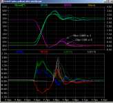
Using Plot in Post 643 http://www.diyaudio.com/forums/attachments/solid-state/685242d1528275513-top-solid-cfa-amp-design-ssahp-kplus-pullout-npre-sim5b-1-5-pre-drivers-png (copied below)
Power transistors are the top plot I(R30) & I(R33). Up to 2.5us the output voltage is negative and R33 (lower power transistor) has the current and is to be turned off next. R30 ramps up while R33 ramps down but goes negative (-0.2A) due to base pull-out current. (Notice R36 and R39 have 0.6A (at 2.7us) which is split into the 3 power transistors base current). So far no undesirable cross-conduction.
Between 2.8us and 2.9us R33 current for the power transistor should go to zero (since only the upper transistor should conduct for 30V output) but there is some ringing caused by the delayed feedback signal via the input stage. R30 shows the lower power transistor is starting to turn on again causing unwanted power transistor cross-conduction (peaking at 0.8A with about 70V across the lower power transistor) ... and the driver stage is a bit slow at changing it's state and the upper driver (NB Q18 in my circuit) stays on while the lower driver (Q19 in my circuit) tries to control the power transistors and this means Q19 has to supply gobs more current, up to 1.8A peak with 70V across it ... quite an ask for a driver transistor even if it is only for 100ns.
Notice the effect of changing the driver transistors base-emitter resistor speeding up the turn off of Q18. EG at 2.85us Q18 has 1A peak cross-conduction with 100 ohm base resistor and no cross-conduction with 25 ohms, and the effect of this is seen in the power transistor cross-conduction reducing from about 0.8A peak to 0.4A peak which is helpful.
I don't know of any DIY amps using this technique that give ppm THD (anyone?Geometric mean biasing is not supposed to solve this cross-conduction issue? If yes, why not to use it, as Bob advised?
 ). I think to match or improve on your circuit using bias control loop it would need even faster driver transistors than what you are using. BTW A nifty biasing loop by Kenpeter (2011) is here Why collector/drain output stages are so rare??? but I haven't simulated it yet and uses common emitter (not common collector) power transistors.
If you have a driver that is as fast as the pre-driver then use it. It seems that drivers are usually slower than pre-drivers (is it due to die size?).If going your way to solve this fenomen, why to use 4 predriver pairs in parallel, while we can use more stiff transistor in a place of predriver like the one used as driver? 4-times power of the predriver, both the same fast.
Last edited:
If I'm not wrong, lowering driver's BE resistor even more provokes higher distortion, despite of multiplying predriver transistors.
If faster transistor means higher FT capable, I never saw such power transistor more faster than currently used.
Predriver and driver transistors are equal in speed in that regard, only cob differs due to die size.
If faster transistor means higher FT capable, I never saw such power transistor more faster than currently used.
Predriver and driver transistors are equal in speed in that regard, only cob differs due to die size.
Last edited:
Ian,4 pre-driver transistors are in parallel with a 10R emitter sharing resistor on each: 4xQ21 are 4x2SC3423 and 4xQ22 are 4x2SC1360.
I did not draw 4 in parallel on the circuit. That may have confused things
The extra base capacitance with 4 pre-driver (pairs) does not seem to affect the PM (approx 57deg).
The THD at 20kHz 15V with 4 pre-drvers reads 4.7ppm vs. 3.1ppm with one driver. Comp 220pF +10R.
The THD at 20kHz 15V with CFP base-base speed-up (50n+10R) and emitter decoupling (1R+68uF) reads 4.1ppm vs. 3.1ppm with no CFP speed-up.
If you wanted CFP speed-up, of the two options I'd take the more conventional paralleling of pre-drivers. A THD of 5ppm at 20kHz is excellent enough
Cheers
I looked at AndriOL's simulation in post 649 according to this at -180 degrees the gain is 14 dB and it doesn't like square wave input with capacitance in parallel with 8R. Rather than put forward a solution for this and add to the confusion, do the current drive enhancements in your circuit improve performance on square wave tests - say 10kHz at 2V input - output load 8R// 1-2uF?
I think not. I tried different value capacitors C12, C24 (1u, 10n, 1n, 600p). Positive power rail deteriorates much faster than negative rail (almost like front end rails) after turn off. Voltage level is 38V for front end, 36V for power section with 4mA input bias current measured with reference to gnd (3.8mA if measured directly). The scope shows the oscillation, but the speaker is dead quiet. Perhaps there is not the source of oscillation where I'm trying to suppress it. Perhaps this is due to too long traces between input and VAS transistors, wider gain bandwidth due to increased bias current of input transistors, which increase the chance of RF ingress or oscillations.It is not clear if you have sorted the front end power supply - what voltage level are the rails at for this test.
I think this is useless to try to make the amp to work with current pcb I have. I'll made the new more compact SE input layout, only than we can estimate if the amp works well. Now we can concentrate on simulation only.
Last edited:
Have you ever considered why this is?If I'm not wrong, lowering driver's BE resistor even more provokes higher distortion, despite of multiplying predriver transistors.
I have routinely increased output transistor emitter values from 0.1R but these always revert in your future simulations. There is a non-linear resistance re between the base and emitter of a transistor and the voltage drop across this will vary. If you imagine the emitter is connected to earth then the signal current and the base voltage will be affected by this. If an external resistor (which is linear) is connected between the emitter and earth most of the voltage will be dropped across this and the impact on the base will be largely swamped in consequence.
You might think of the value of the emitter resistor value in terms of the length of studs on winter sports foot-wear. I suggest you read what Bob Cordell had to say in post 293 on page 30.
Originally Posted by IanHegglun
The THD at 20kHz 15V with CFP base-base speed-up (50n+10R) and emitter decoupling (1R+68uF) reads 4.1ppm vs. 3.1ppm with no CFP speed-up.
Thank you dear IanHegglun for this trick. On simulation it also helps CFP as output.
Gratefully yours,
M.
Stopping oscillations by temporarily increasing the feedback resistor
The trick is to raise the feedback resistance in stages until it stops oscillating. First stage try doubling R19,R20 (eg lift one end of R19 & R20 and add another of the same value). This doubles the gain of the amp (but it is only a temporary step) and it halves the amount of feedback. Since it is usually an oscillation from feedback this will eventually stop the feedback by reducing the amount of feedback enough.
If the amp is still oscillating then increase R19 & R20 by a factor of 4 (eg add 4k7 in series with the original R19 & R20). Eventually the feedback will be reduced enough to stop oscillations.
Then, once it is stable you can change compensation capacitor values to learn what they are affecting, like squarewave recovery, and from that you can restore more feedback until you get back to the original feedback resistors without oscillations.
Also, in simulations using the same component values as your PCB amp you can see any differences in the squarewave tests, and then you adjust you simulation to make it do what your PCB amp does. Then you can use simulations to probe PM and GM with different modifications that are hard to do with bench testing.
Cheers
Andriy, don't give up on the present PCB just yet because there is one sure way to stop oscillations that you can use....I think this is useless to try to make the amp to work with current pcb I have. I'll made the new more compact SE input layout, only than we can estimate if the amp works well. Now we can concentrate on simulation only.
The trick is to raise the feedback resistance in stages until it stops oscillating. First stage try doubling R19,R20 (eg lift one end of R19 & R20 and add another of the same value). This doubles the gain of the amp (but it is only a temporary step) and it halves the amount of feedback. Since it is usually an oscillation from feedback this will eventually stop the feedback by reducing the amount of feedback enough.
If the amp is still oscillating then increase R19 & R20 by a factor of 4 (eg add 4k7 in series with the original R19 & R20). Eventually the feedback will be reduced enough to stop oscillations.
Then, once it is stable you can change compensation capacitor values to learn what they are affecting, like squarewave recovery, and from that you can restore more feedback until you get back to the original feedback resistors without oscillations.
Also, in simulations using the same component values as your PCB amp you can see any differences in the squarewave tests, and then you adjust you simulation to make it do what your PCB amp does. Then you can use simulations to probe PM and GM with different modifications that are hard to do with bench testing.
Cheers
Last edited:
- Status
- This old topic is closed. If you want to reopen this topic, contact a moderator using the "Report Post" button.
- Home
- Amplifiers
- Solid State
- One of the Top Solid-State CFA amp design