I'm not strong in formulas and mathematics. What is the conclusion than for those who don't use thermaltracks? If to use 0.22R Re, what about Roender's FC-100 amp where he found the most optimal Re is 0.1R XOD wise with matched output devices (0.22R for not perfectly matched OPs).
You're best bet is to to build it with real devices and observe the effects of different biases and values.
I can't fine a nice tutorial on the geometric mean biasing right now. There was an IC version by National or LT (LT1166) that was to be used with external output devices. The data sheet might be of help in explaining.
Last edited:
Driver pull-out current issues
As for non-switching circuits I can't get them to slew safely at anywhere near the speeds of most amps today and this means worse dynamic XOD. I developed a charge pull-out method for my CSD (Current Source Driven power stage) amp which included a non-switching bias. One problem I had with the pull-out circuit is the capacitors to remove transient base current can be adjusted to work for normal loads but isn't right for no-load or vice versa since charge changes with load current. It appears that the charge pull-out process needs to be under very-fast negative feedback to work well with different loads -- and that's one reason why the Locanthi-T arrangement works well.
Now to AndriyOL's amp. I found the SSAHP pull-out current can go as high as 1A with a 4 ohm load and 100ns rise-fall time squarewave. The circuit I used (sim5) has a Locanthi-T resistor of 12 ohms giving a driver bias current of 120mA and each driver dissipates 4W, nearly as much as each of the 3 power transistors idle dissipation.
This gives 700V/us slew-rate that is high enough to deliberately provoke cross-conduction to analyse what is going on, and then to see if cross-conduction can be reduced. Note: with a rise/fall time of 500ns the cross-conduction currents are well controlled and safe and peak pull-out base currents are then 300mA.
There is also a shunt R+C (0.8R+1uF) across the Locanthi-T resistor which provides 10 times the peak pull-out currents than just a 12 ohm resistor because the Locanthi-T resistor swings about 1.2V swing and with 12 ohms the pull-out current is limited to 100mA.
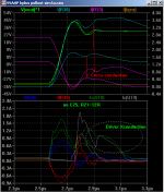
See the first attached plot for the original (Sim5a attached) showing:
Top traces, the power transistor emitter currents (one of 3 in parallel),
Bottom traces, the driver transistor currents (Q18 upper driver). R36,R39 are the net base currents to the power transistors (R36 upper, +ve is pull-out current).
The tail region has ringing with a protracted time of cross-conduction (300ns) in the power transistors (1A) and also the driver transistors (1A) -- again this only occurs when the squarewave rise/fall times are less than 300ns.
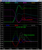
The second attached plot shows the effect on the cross-conduction currents when the Locanthi-T resistor (R21) is increased to 24 ohms (by opening jumper X1). The driver cross-conduction currents in the tail end is reduced slightly, not increased as might be expected. So does this resistor need to be so low? And what is the cause of the drivers' cross-conduction anyway?
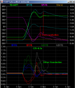
The third attached plot shows the effect on the cross-conduction currents with the same 24 ohm Locanthi-T resistor but now a capacitor (C25 0.2uF) is added to couple the two bases of the CFP driver transistors (Q18,Q19). I know this is not recommended due to power rail ripple injection, but it serves to uncover the main reason for the drivers' cross-conduction. Both the driver's and power transistors' cross-conduction reduces with this capacitor due to faster charge pull-out of the driver's. Notice the two base currents are now working as opposite phase. There is still some cross-conduction in the driver currents but is less and decays faster with C25 added.
AndriyOL, it would be nice to be able to add C25 to speed up the CFP transistor's turn-off and greatly reduce the problem of driver and power transistor turn-off for worst case situations when bench testing to see what it can do. To add this capacitor C25 I suggest that there would need to be a 1uF//10nF decoupling capacitor pair directly from the pos-neg rail and wired as close as possible to the drivers emitters, plus a 10R in series with C25 and driver base-emitter protection diodes (1A fast). It could be worth trying and if it doesn't help then Plan B is to increase the compensation to remove the ringing and/or use an input filter with a rise-time of more than 0.5us.
Bob, I hope this is of some use to you even though this CFP driven triple is rarely used with some hard to design twists, including the shunt R+C across the Locanthi-T resistor, which can be problematic, but here it does significantly increase the pull-out current -- but requires driver transistors that can swing in 10's of nanoseconds -- and if the drivers are not able to turn-off ultra-fast then driver (and power...) transistor cross-conduction occurs with low-R loading and very-fast rise/fall slewing.
Cheers
Thanks Bob. Sorry about the delay. I did some simulations of the SSAHP circuit looking the pull-out current and cross-conduction....
Dynamic XOD is a different beast, and it is important not to confuse it or its symptoms with static XOD. Dynamic XOD is related to turning the output transistors on and off sufficiently fast as output current changes rapidly at high frequencies when the output current passes through zero. It is also called switching distortion. It mainly has to do with the rate of change of output current, or current slew rate. The most significant source of dynamic XOD or switching distortion is the inability to switch off quickly an output transistor that has been conducting a large amount of current. This results from not enough ability to suck out minority carriers from the base. In most output stage arrangements, turning the output transistor on sufficiently fast is much less of a problem.
The most straightforward and effective way to reduce dynamic (switch-off) XOD is to be able to provide a sufficiently high pull-out current from the base of the output transistor. The required amount of current is proportional to the output current slew rate and inversely proportional to the ft of the output device.
In a Locanthi Triple, for example, running the driver transistors with a high bias current, on the order of 30-60 mA or more, largely solves this problem. In simulation, look at the collector current of the driver transistor under conditions of high output current swing at high frequencies (e.g., full power into a 4-ohm or 2-ohm load at frequencies of at least 20 kHz). It should never go to zero. If it goes to zero, the driver has lost control of the output transistor.
...
Cheers,
Bob
As for non-switching circuits I can't get them to slew safely at anywhere near the speeds of most amps today and this means worse dynamic XOD. I developed a charge pull-out method for my CSD (Current Source Driven power stage) amp which included a non-switching bias. One problem I had with the pull-out circuit is the capacitors to remove transient base current can be adjusted to work for normal loads but isn't right for no-load or vice versa since charge changes with load current. It appears that the charge pull-out process needs to be under very-fast negative feedback to work well with different loads -- and that's one reason why the Locanthi-T arrangement works well.
Now to AndriyOL's amp. I found the SSAHP pull-out current can go as high as 1A with a 4 ohm load and 100ns rise-fall time squarewave. The circuit I used (sim5) has a Locanthi-T resistor of 12 ohms giving a driver bias current of 120mA and each driver dissipates 4W, nearly as much as each of the 3 power transistors idle dissipation.
This gives 700V/us slew-rate that is high enough to deliberately provoke cross-conduction to analyse what is going on, and then to see if cross-conduction can be reduced. Note: with a rise/fall time of 500ns the cross-conduction currents are well controlled and safe and peak pull-out base currents are then 300mA.
There is also a shunt R+C (0.8R+1uF) across the Locanthi-T resistor which provides 10 times the peak pull-out currents than just a 12 ohm resistor because the Locanthi-T resistor swings about 1.2V swing and with 12 ohms the pull-out current is limited to 100mA.
See the first attached plot for the original (Sim5a attached) showing:
Top traces, the power transistor emitter currents (one of 3 in parallel),
Bottom traces, the driver transistor currents (Q18 upper driver). R36,R39 are the net base currents to the power transistors (R36 upper, +ve is pull-out current).
The tail region has ringing with a protracted time of cross-conduction (300ns) in the power transistors (1A) and also the driver transistors (1A) -- again this only occurs when the squarewave rise/fall times are less than 300ns.
The second attached plot shows the effect on the cross-conduction currents when the Locanthi-T resistor (R21) is increased to 24 ohms (by opening jumper X1). The driver cross-conduction currents in the tail end is reduced slightly, not increased as might be expected. So does this resistor need to be so low? And what is the cause of the drivers' cross-conduction anyway?
The third attached plot shows the effect on the cross-conduction currents with the same 24 ohm Locanthi-T resistor but now a capacitor (C25 0.2uF) is added to couple the two bases of the CFP driver transistors (Q18,Q19). I know this is not recommended due to power rail ripple injection, but it serves to uncover the main reason for the drivers' cross-conduction. Both the driver's and power transistors' cross-conduction reduces with this capacitor due to faster charge pull-out of the driver's. Notice the two base currents are now working as opposite phase. There is still some cross-conduction in the driver currents but is less and decays faster with C25 added.
AndriyOL, it would be nice to be able to add C25 to speed up the CFP transistor's turn-off and greatly reduce the problem of driver and power transistor turn-off for worst case situations when bench testing to see what it can do.
To add this capacitor C25 I suggest that there would need to be a 1uF//10nF decoupling capacitor pair directly from the pos-neg rail and wired as close as possible to the drivers emitters, plus a 10R in series with C25 and driver base-emitter protection diodes (1A fast). It could be worth trying and if it doesn't help then Plan B is to increase the compensation to remove the ringing and/or use an input filter with a rise-time of more than 0.5us.Bob, I hope this is of some use to you even though this CFP driven triple is rarely used with some hard to design twists, including the shunt R+C across the Locanthi-T resistor, which can be problematic, but here it does significantly increase the pull-out current -- but requires driver transistors that can swing in 10's of nanoseconds -- and if the drivers are not able to turn-off ultra-fast then driver (and power...) transistor cross-conduction occurs with low-R loading and very-fast rise/fall slewing.
Cheers
Attachments
Optimized CFP speed-up capacitor
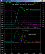
A bit more simulation to optimization of C25 gives 50nF +10 ohms when the Locanthi-T resistor is 24 ohms. I also found adding 2R2 degeneration resistors in the drivers helps to reduce cross-conduction.

The attached plot shows driver current and base currents are now well controlled with no driver cross-conduction with 4 ohms load, a 100ns input step and the same compensation as before. Now with only 50nF +10R between the driver bases the danger of damaging the bases is probably not an issue and power rail ripple injection is quite small at 20kHz.

So it looks to me like a worthwhile modification unless someone can show why it should not be used.
Cheers
...AndriyOL, it would be nice to be able to add C25 to speed up the CFP transistor's turn-off and greatly reduce the problem of driver and power transistor turn-off for worst case situations ...
A bit more simulation to optimization of C25 gives 50nF +10 ohms when the Locanthi-T resistor is 24 ohms. I also found adding 2R2 degeneration resistors in the drivers helps to reduce cross-conduction.
The attached plot shows driver current and base currents are now well controlled with no driver cross-conduction with 4 ohms load, a 100ns input step and the same compensation as before. Now with only 50nF +10R between the driver bases the danger of damaging the bases is probably not an issue and power rail ripple injection is quite small at 20kHz.
So it looks to me like a worthwhile modification unless someone can show why it should not be used.
Cheers
Attachments
I tried recently to modify the circuit with current pcbs I have. I changed driver's bias current and installed 195p+10R compensation , however the amp is not quite stable. I was able to bias input transistors only to 3mA first time (than only to 2mA second time) and 2mA second channel with diodes string output bias, when I swapped the channels for one PSU used. Perhaps this is due to PCB layout influences. Than will try your mod Ian with 50nF +10R between the driver bases.
When I try to increase input bias current over 31mV drop on 10R emitter resistors I got sudden surge increase of output bias current. Also Q16, Q18 getting very hot which isn't safe for them to be operated without heatsink. I'm using Zobel network on the out, bulb tester for both PSUs (33/43VDC currently) connected in parallel. Will try to power front end psu directly.
Installing RC filter on drivers' bases don't help, as well as powering front end psu directly.
Output bias current getting lower and the amp is stabilized when I measure V drop at input emitter resistors or direct an airflow on input and VAS TO-126 transistors. Maybe this is a thermal runaway of input or VAS transistors?
What do you mean by "and driver base-emitter protection diodes"? Could you please write\show which diode and how to connect it?To add this capacitor C25 I suggest that there would need to be a 1uF//10nF decoupling capacitor pair directly from the pos-neg rail and wired as close as possible to the drivers emitters, plus a 10R in series with C25 and driver base-emitter protection diodes (1A fast).
When I try to increase input bias current over 31mV drop on 10R emitter resistors I got sudden surge increase of output bias current. Also Q16, Q18 getting very hot which isn't safe for them to be operated without heatsink. I'm using Zobel network on the out, bulb tester for both PSUs (33/43VDC currently) connected in parallel. Will try to power front end psu directly.
Installing RC filter on drivers' bases don't help, as well as powering front end psu directly.
Output bias current getting lower and the amp is stabilized when I measure V drop at input emitter resistors or direct an airflow on input and VAS TO-126 transistors. Maybe this is a thermal runaway of input or VAS transistors?
The required amount of current is proportional to the output current slew rate and inversely proportional to the ft of the output device.
Bob
Bob I understand the principal from this statement but I'm having difficulty extracting a formula for calculating the driver static current from the output current slew rate. Can you put up a formula so I can rap my head around this.
What you are describing here sounds a lot like what Pete (PBS) described as cross conduction in the output transistors at the crossover point. Can you confirm that cross conduction and dynamic XOD are one and the same?
Cheer,
R44/C25 will cause rectifier pulses and load surges from the output transistors to modulate the driver slaves. This could have variable unintended consequences depending on board layout. If you do this I would suggest feeding the driver section with an RC to reduce the influence of the output transistors on it's supply voltage.
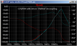
PS decoupling for CFP speed-up C25/R44
Do you have a 1st time power up procedure from previous days, eg, from LC etc?
I would have thought you would start with the output stage disabled by shorting the Vbe multiplier (since you don't have a bias trimpot, or do you?). Then with a dummy load and (hopefully) 0V on the output you first get the input stage current to 3mA on both sides and then get the VAS to 15mA to 20mA range. When that's OK then remove the Vbe multiplier short starting from a low current region, and set the Vbe voltage to get the right idle current and check if the idle current is settling when warming up. Then if the amp is not oscillating at any frequency including RF, then check the DC on the output and trim if necessary, then apply an input signal starting from a low level.
Keantoken's concern (Post 626) is "rectifier pulses and load surges from the output transistors to modulate the driver slaves" so I did a simulation to check the PSRR 1) before adding C25/R44 (50nF +10R) between the driver bases, and 2) with C25/R44. At 20kHz there is 30dB less PSRR (first attached plot).
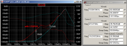
To get the PSRR back the same as without C25/R44 I added 1 ohm resistors in the emitters of the drivers and ran another cross-rail capacitor (C26). without C25/R44 is the minimum needed to stop the PSRR being degraded (second plot). The third plot shows the circuit.
The last plot shows the difference of cross-conduction with and without without C25/R44 and with 1R/68uF decoupling (as previous post worst case with 4 ohms and 100ns input step, and two 220pF+10R comp).
Notice, in particular, how the power transistor turn-off tail is reduced (IR33), simply by making the drivers turn off faster with less driver cross-conduction.
If this works in practice then it means it is not necessary to stop the ringing by using more compensation, nor is it necessary to add an input filter to keep the slew rate low enough to stop excessive cross-conduction. If this works in practice it should be safe enough to test your amp into 4 ohms and drive it to the rails at 100kHz, something that few bipolar power amps can do without overheating from cross-conduction. Here's for hoping.
Cheers
I can't follow all your tests; so I can't tell if you got it biased right.I tried recently to modify the circuit with current pcbs I have. I changed driver's bias current and installed 195p+10R compensation , however the amp is not quite stable. I was able to bias input transistors only to 3mA first time (than only to 2mA second time) and 2mA second channel with diodes string output bias, when I swapped the channels for one PSU used. Perhaps this is due to PCB layout influences.
...
When I try to increase input bias current over 31mV drop on 10R emitter resistors I got sudden surge increase of output bias current. Also Q16, Q18 getting very hot which isn't safe for them to be operated without heatsink. I'm using Zobel network on the out, bulb tester for both PSUs (33/43VDC currently) connected in parallel. Will try to power front end psu directly.
Installing RC filter on drivers' bases don't help, as well as powering front end psu directly.
Output bias current getting lower and the amp is stabilized when I measure V drop at input emitter resistors or direct an airflow on input and VAS TO-126 transistors. Maybe this is a thermal runaway of input or VAS transistors?
Do you have a 1st time power up procedure from previous days, eg, from LC etc?
I would have thought you would start with the output stage disabled by shorting the Vbe multiplier (since you don't have a bias trimpot, or do you?). Then with a dummy load and (hopefully) 0V on the output you first get the input stage current to 3mA on both sides and then get the VAS to 15mA to 20mA range. When that's OK then remove the Vbe multiplier short starting from a low current region, and set the Vbe voltage to get the right idle current and check if the idle current is settling when warming up. Then if the amp is not oscillating at any frequency including RF, then check the DC on the output and trim if necessary, then apply an input signal starting from a low level.
Actually, after reducing the value of C25 to 50nF and adding 10 ohms, these diodes can probably be safely omitted.Then will try your mod Ian with 50nF +10R between the driver bases.
What do you mean by "and driver base-emitter protection diodes"? Could you please write\show which diode and how to connect it?
Keantoken's concern (Post 626) is "rectifier pulses and load surges from the output transistors to modulate the driver slaves" so I did a simulation to check the PSRR 1) before adding C25/R44 (50nF +10R) between the driver bases, and 2) with C25/R44. At 20kHz there is 30dB less PSRR (first attached plot).
To get the PSRR back the same as without C25/R44 I added 1 ohm resistors in the emitters of the drivers and ran another cross-rail capacitor (C26). without C25/R44 is the minimum needed to stop the PSRR being degraded (second plot). The third plot shows the circuit.
The last plot shows the difference of cross-conduction with and without without C25/R44 and with 1R/68uF decoupling (as previous post worst case with 4 ohms and 100ns input step, and two 220pF+10R comp).
Notice, in particular, how the power transistor turn-off tail is reduced (IR33), simply by making the drivers turn off faster with less driver cross-conduction.
If this works in practice then it means it is not necessary to stop the ringing by using more compensation, nor is it necessary to add an input filter to keep the slew rate low enough to stop excessive cross-conduction. If this works in practice it should be safe enough to test your amp into 4 ohms and drive it to the rails at 100kHz, something that few bipolar power amps can do without overheating from cross-conduction. Here's for hoping.
Cheers
Attachments
-
 SSAHP kplus sim5b CFPmod decoupling 100n-step 4R.png17.1 KB · Views: 146
 -
 SSAHP kplus sim5b CFPmod decoupling cct.png21.7 KB · Views: 140
 -
 SSAHP kplus sim5b CFPmod decoupling PSRR.png10.9 KB · Views: 245
 -
 SSAHP kplus sim5b CFPmod PSRR.png20.1 KB · Views: 277
 -
SSAHP kplus sim5b CFPmod 100n step.zip7.8 KB · Views: 52
Hi keantoken,R44/C25 will cause rectifier pulses and load surges from the output transistors to modulate the driver slaves. This could have variable unintended consequences depending on board layout. If you do this I would suggest feeding the driver section with an RC to reduce the influence of the output transistors on it's supply voltage.
Thanks. See Post 627, it covers PSRR tests and a way to filter the rails so PSRR is not degraded by C25/R44.
Cheers
Do you have a 1st time power up procedure from previous days, eg, from LC etc?
I would have thought you would start with the output stage disabled by shorting the Vbe multiplier (since you don't have a bias trimpot, or do you?).
I have the bias trimpots: two 100R for IPS bias and one 500R for OPS bias.
I thought if I'm not driving the amp to clipping I don't need dummy load, just cheap 4ohm speaker and simple light bulb tester. At least I can hear something from the speaker when compared to dummy load. Btw, I have a variac if it's required for testing.
Output DC offset is 0-10mV when stabilized. VAS bias current is 89mV drop or 8.9mA with input bias current 31.5mV or 3.1mA. OPS bias trimpot is set to maximum value 500R. PSUs during measurements were 35\45VDC. Perhaps my OPS trimpot is too low in value, it must be 2K at least, according to simulation.
How to get VAS bias current higher?
That sounds like you doing a good job of working through the initial power up testing.
A variac is nice for the very first time you power up the power supply and amp connected to the PSU.
A cheap speaker with a series lamp is an excellent idea to listen for abnormalities.
The VAS current was about 19mA on the latest sims and yours is 9mA. This reduces the output stage bias top end range. So try and increase the VAS current by increasing the input current slightly.
For initial power up testing of the power stage idle current you could connect a second temporary trimpot in series with the present Vbe multiplier one (a second 5k trimpot) to give a lower minimum idle current. Once the amp is biasing properly you can remove the second trimpot.
Cheers
There is quite a lot of added complexity in the circuit. The most straight forward way to deal with the base charges in the outputs is to get the CFP units to work independently in push-pull this is not happening because the first transistor in each CFP receives a emitter signal from the second and from the cross-coupling to the opposite half CFP.
Who would not have trouble listening to three conversations at once.
In short the first transistors in each CFP need a resistor inserted from its emitter to the collector of the second transistor. The cross -coupling between output halves needs to be fixed at the collectors of the second transistors in each CFP pair.
The attached simulation illustrates how this is was done by a well respected manufacturer.
Attachments
Mjona,There is quite a lot of added complexity in the circuit. ....
The attached simulation illustrates how this is was done by a well respected manufacturer.
Thanks. I tried adding your 15 ohm resistors in the emitters of the pre-driver of the CFP and the 2R2's in the emitters of the drivers and without my C25.
Cross-conduction peaks in the driver's are not reduced and the recovery time is lengthened.
Maybe the 15 ohm resistors in the emitters of the pre-driver's that you saw were for solving a different issue of the CFP?
Cheers
My previous post about 500 Ohms value at trimpot on pcb was not correct. In fact the trimpot value was 0 Ohm, that's why I had rapid current consumption after reaching 3mA input bias current or setting the trimpot to higher resistance from zero.
When I changed the current 500R trimpot to 2K, set the maximum value, the output bias started to rise even with 2mA input bias current.
With 2.9mA input bias, 2k trimpot value, I have 13.5mV on output emitters, 52mV on VAS emitters, 29V\37.5V on PSUs. My highest value 150W bulb tester isn't enough, as voltage drops further if to rise input bias higher, heatsink is almost hot, I think it won't handle 160-200mA output bias. Will try to change the trimpot to 10K and connect main PSU DC rails via 20 Ohms 20W serial resistors.
Last edited:
My previous post about 500 Ohms value at trimpot on pcb was not correct. In fact the trimpot value was 0 Ohm, that's why I had rapid current consumption after reaching 3mA input bias current or setting the trimpot to higher resistance from zero.
When I changed the current 500R trimpot to 2K, set the maximum value, the output bias started to rise even with 2mA input bias current.
With 2.9mA input bias, 2k trimpot value, I have 13.5mV on output emitters, 52mV on VAS emitters, 29V\37.5V on PSUs. My highest value 150W bulb tester isn't enough, as voltage drops further if to rise input bias higher, heatsink is almost hot, I think it won't handle 160-200mA output bias. Will try to change the trimpot to 10K and connect main PSU DC rails via 20 Ohms 20W serial resistors.
The serial resistor idea is a good one. I have used this method although I start with 100R and try other values depending on what I find. I use a meter on dc range with the probes in the output terminals and in a place where I can see it at a glance.
A moistened finger is a useful way to sense drafts and heat so I have a trusty pinky near a serial resistor and my other free hand on the on/off switch ready to react quickly if necessary.
From what you have reported the dc offset should be Ok.
The amplifier could be unstable with lower voltage rails as this will affect transistor bias voltages but it is a better policy to check rather than assume. This is why I suggested starting with higher value serial resistors and working down in value.
While you have not been able to adjust the Iq to full value it is important to know that whatever adjustment you have is smooth and proportional to the movement.
There would appear to be a point where the movement and change become disproportionate. It would be better to reduce the Iq to a low value and increase it at intermediate steps with difference serial resistors in the supply lines.
A small movement of a 10k trimmer will result in a larger change in track resistance which could make fine adjustment more finnicky in the long run.
I think you should leave that until closer to the end of the process. If 10k is necessary and adjustment does turn out to be finnicky you could solder a resistor across the ends under the board.
After a change to 10K trimpot, when I reach 4mA input bias (it's different to 0.3-0.4mA when to measure with reference to GND or directly on the resistors), front end psu sags to 20V, VAS heatsink which I installed is quite hot, VAS bias was 226mV.
As I can see, VAS transistors consume too much current, they are very hot without heatsinks. Optimal input bias for not to sag front end rails is 3.1-3.2mA. Positive rail is little bit unstable, front end LED blinks lightly when I touch the components, and output LED extincts much faster than negative rail LED.
As I can see, VAS transistors consume too much current, they are very hot without heatsinks. Optimal input bias for not to sag front end rails is 3.1-3.2mA. Positive rail is little bit unstable, front end LED blinks lightly when I touch the components, and output LED extincts much faster than negative rail LED.
Last edited:
If you are still using the light bulb test set up the transistor biasing voltages will be out of kilter everywhere.
I looked at the CFP emitter currents for your circuit at 16 volts peak out and noted something odd with Q18 and Q19 voltage levels.

The test signal was at 20 kHz.
The modified CFP equivalent is attached. I have made a couple of changes to improve the symmetry - increasing the output transistor emitters to 0.33R and decreasing the Iq to reduce heat dissipation - an issue which AndriyOL is becoming concerned over.

Mjona,
Thanks. I tried adding your 15 ohm resistors in the emitters of the pre-driver of the CFP and the 2R2's in the emitters of the drivers and without my C25.
Cross-conduction peaks in the driver's are not reduced and the recovery time is lengthened.
Maybe the 15 ohm resistors in the emitters of the pre-driver's that you saw were for solving a different issue of the CFP?
Cheers
I looked at the CFP emitter currents for your circuit at 16 volts peak out and noted something odd with Q18 and Q19 voltage levels.
The test signal was at 20 kHz.
The modified CFP equivalent is attached. I have made a couple of changes to improve the symmetry - increasing the output transistor emitters to 0.33R and decreasing the Iq to reduce heat dissipation - an issue which AndriyOL is becoming concerned over.
If you are still using the light bulb test set up the transistor biasing voltages will be out of kilter everywhere.
I found out I only have 2 x 20R 20W resistors, which isn't a perfect choice for such testing.
The front end voltage sags not because of I'm using bulb tester. Output voltage is normal, but front end sags too much. If the reson was bulb tester it would sags both voltages.
With 15mA VAS, 3.6mA input bias PSU voltages are 37V at output and 40V at front end, should be 37\47. Emitter volatges at Q16, Q17 with ref to gnd are 35.9, 35.6V
Last edited:
I think sim currents are wrong. For example, Spice only shows 0.5W Pd for Q16, Q17 which should be only little warm with such level of dissipation, however even big copper heatsink for those transistors is hot.
I tested front end psu before, it can easily withstand 1-2A load. Transformer has 40VA, 37-0-37VAC
I tested front end psu before, it can easily withstand 1-2A load. Transformer has 40VA, 37-0-37VAC
Last edited:
- Status
- This old topic is closed. If you want to reopen this topic, contact a moderator using the "Report Post" button.
- Home
- Amplifiers
- Solid State
- One of the Top Solid-State CFA amp design