As I wrote, It is not possible to control gain via P1 in posted circuit.
Look the schematic here http://www.diyaudio.com/forums/solid-state/235695-no-nfb-line-amp-gainwire-mk2-9.html#post3579816, it could be confusing as there are two P1 at the input and other one not used as pot in case of ODNF.
I suggest that this version of the GainWire mk2 with +-15V power supply will be used to design PCB. In this case no need for separate power supply for the op amp and the pre amp did not loose any of the driving possibilities.
I suggest also that the 10k input pot(P1) will be used as with 100k pot distortion raises ten times then with the 10k pot. This is the situation when the pot is in the midle setting and prevailed distortion is input distortion(at least in simulation).
Total current consumption is a bit less then 40mA.
BR Damir
Hi dadod
I really like your schematic and I Wonder if I could use it as a riaa stage (replacing R19 with a passive riaa eq filter).... Maybe I would need more gain, but that could be done modding imput stage right ?
ODNF gainloop, the gain plots and asc zip file.
Thanks, had to take out the references to dadomodels.txt and supertex.txt but it runs now.
")
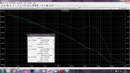
LTspice calculates THD at 1kHz as 0.000000%
Not enough digits after the decimal point? First time I've seen that!
Even at 20kHz THD is 0.000004%.
Very nice.
Last edited:
Hi dadod
I really like your schematic and I Wonder if I could use it as a riaa stage (replacing R19 with a passive riaa eq filter).... Maybe I would need more gain, but that could be done modding imput stage right ?
It's not that simple, R19 does not define the gain, P1/R9 does, R19 is a part of the compensation. I am not sure if this gain block could be used in RIAA stage, probably with some changes it could.
I was wondering if this topology could be used to make a power amp. First order of business is more gain. Tweaking P1/R9 did not give a lot more. Dropping R38 to 470 ohm made things came alive. I then upped the input to 1V and observed this very gentle clipping behaviour - almost valve-like. An unexpected bonus. 
Attachments
I was wondering if this topology could be used to make a power amp. First order of business is more gain. Tweaking P1/R9 did not give a lot more. Dropping R38 to 470 ohm made things came alive. I then upped the input to 1V and observed this very gentle clipping behaviour - almost valve-like. An unexpected bonus.
Yes it could be used, look here http://www.diyaudio.com/forums/solid-state/238252-odnf-no-gnfb-power-amp.html#post3539335
Damir, you may want to move the caps and other components around U1 a little away from U1 - my existing layout for the discrete opamp is about 15.2 x 15.2 mm (i.e. a little bigger on all sides than DIP8 monolithics).
Here I moved some components away from op amp socket, I hope it's enough space now.
BR Damir
Attachments
![GainWire-mk2-32_300-ODNF.LAY].jpg](/community/data/attachments/332/332403-9fe8bbcbd4b1b61b87833c32692d2c27.jpg)
What sets the bias to zero volts at the collectors of Q6 and Q8 ? Will it stay at zero when you use real transistors that dont all have identical parameters as in the sim? Change the Early voltage of Q6 by 10% and see what happens.
The op amp will set output DC voltage to zero(it acts as DC servo too) and the collectors of Q6 and Q8 will not probably stay at zero.
The op amp will set output DC voltage to zero(it acts as DC servo too) and the collectors of Q6 and Q8 will not probably stay at zero.
So wont this be a problem with real circuits?
So wont this be a problem with real circuits?
I don't see why.
![GainWire-mk2-32_300-ODNF-b.LAY].jpg](/community/data/attachments/336/336937-7349ed8d992230addd67217cfe988fe3.jpg)
![GainWire-mk2-32_300-ODNF-DS.LAY].jpg](/community/data/attachments/336/336938-c9bf48b767f13f821f3ef2e6a4765763.jpg)
Two proposed PCBs, single side and double side. Corrected some mistakes.
Dimension 115x50 mm.
BR Damir
Thanks, Damir.
My only concern (not a show-stopper) is that the ground is not a star ground, and has lots of taps along its length. Perhaps it could be reworked into a single-point star ground, close to the centre of the board?
I'm not too intuitively familiar with the topology and its large-current flows, to be able to give specific suggestions, but it looks fine otherwise.
There are actually two separated grounds, input groung(gnd) and power ground(GND). I thought to connect those grounds to outside star ground where all grounds will join, power supply too from the power supply unit.
Thanks linuxguru!
BR Damir
So if the dc bias voltage at the collectors of Q6 and Q8 is -12 volts, thats not a problem?I don't see why.
So if the dc bias voltage at the collectors of Q6 and Q8 is -12 volts, thats not a problem?
Why it would be -12V, it will be just enough to set output DC close to zero.
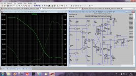
Damir,
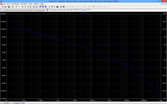
This is the open loop gain and phase margin of your circuit.
Unfortunately it does not have the minimum phase margin of 60º, and it has less than 30º at 1Mhz , the problem is caused by the P1 (10k) .
This is the open loop gain and phase margin of your circuit.
Unfortunately it does not have the minimum phase margin of 60º, and it has less than 30º at 1Mhz , the problem is caused by the P1 (10k) .
Attachments
Last edited:
Damir,
This is the open loop gain and phase margin of your circuit.
Unfortunately it does not have the minimum phase margin of 60º, and it has less than 30º at 1Mhz , the problem is caused by the P1 (10k) .
I don't know why you call it open loop gain and how you simulated it, but here is my simulation of the loop gain. Phase margin is 70degree, and gain margin is 20dB.
Attachments
- Status
- This old topic is closed. If you want to reopen this topic, contact a moderator using the "Report Post" button.
- Home
- Amplifiers
- Solid State
- No NFB line amp (GainWire mk2)