@ dadod
Congratulations, after a long, long search . . . . for a natural sound")
Best transconductance propagation ever seen
You ''Nail it''
Now only to a real life . . . .
My best regards,
Andreas


Thank you Andreas,
BR Damir
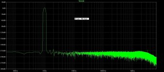
1kHz 2 V output on 10k load!!!!
Oh sorry I forgot to mention all that with just +-15V of the power supply!
This is realy GainWire
Move over and retire the blowtorch Mr Curl
What is the gain, I want to get an idea of input refered noise.
Can you post the asc file.
Maybe we can get Linuxguru to supply discrete opamps for the ODNF.
I think some members are going to complain that the design cannot possibly sound good because it doesnt have harmonic distortion
The gain is P1/R9 and in this case it is 5.55.
I will post asc file later.
What is the gain, I want to get an idea of input refered noise.
Can you post the asc file.
Manso, have you done some simulation? Any suggestion?
BR Damir
I was just thinking, maybe in the future, if there is interest to offer PCB???
There is very much interest in pcb for this fine amp design. I just got my Audio-Precision 2722 analyzer today and so can mesure it to compare with SIM.
Thx-RNMarsh
There is very much interest in pcb for this fine amp design. I just got my Audio-Precision 2722 analyzer today and so can mesure it to compare with SIM.
Thx-RNMarsh
Thenks Richard for your opinion.
OK I will push myself to do the PCB, but still I appreciate a help here.
BR Damir
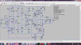
+-15V version
I suggest that this version of the GainWire mk2 with +-15V power supply will be used to design PCB. In this case no need for separate power supply for the op amp and the pre amp did not loose any of the driving possibilities.
I suggest also that the 10k input pot(P1) will be used as with 100k pot distortion raises ten times then with the 10k pot. This is the situation when the pot is in the midle setting and prevailed distortion is input distortion(at least in simulation).
Total current consumption is a bit less then 40mA.
BR Damir
Attachments
![GainWire-mk2-32_300-ODNF.LAY].jpg](/community/data/attachments/329/329107-07a54c37d2243fd38f0561dfa0c8c0df.jpg)
![GainWire-mk2-32_300-ODNF.LAY].jpg](/community/data/attachments/331/331061-49d0d760bcf1ba6471866dbca6487f34.jpg)
???No NFB line amp
U1 is in signal path ("nested" NFB, U1 is comparing input vs. output with fixed gain, with correction at lower P1 side, that is why this circuit is not sensitive to load) , whole performance is dictated by U1 (ideal?) parameters. It is not possible to control gain via P1, try it, U1 will compensate any attempt to vary gain..
Here is the PCB, suggestion welcome. Dimension 110x50 mm.
BR Damir
Damir, you may want to move the caps and other components around U1 a little away from U1 - my existing layout for the discrete opamp is about 15.2 x 15.2 mm (i.e. a little bigger on all sides than DIP8 monolithics).
I have PCBs for a previous version of the LF06/FET990 (which doesn't implement the LTP Wilson current mirror, the VAS bootstrapped clamp or the Diamond Cascode at the output), and it is tested and works ok, but THD20 will not be as low as the current version (for which the layout is completed and fits in the same 15.2 x 15.2 mm, but still awaiting some tweaks and DRC before giving it for fabrication). The Diamond Cascode has also been tested separately as an opamp current-booster for monolithic single opamps, and it seems to work as per the simulation.
If there's interest in the previous version PCB and/or kits, please PM me. I would also appreciate a good source for authentic BF862 JFETs in moderate quantities (200 to 500 pieces). I'm currently using Toshiba 2sk209-BL for the input LTP, and it works, but probably has lower Yfs and Idss than the BF862.
???
U1 is in signal path ("nested" NFB, U1 is comparing input vs. output with fixed gain, with correction at lower P1 side, that is why this circuit is not sensitive to load) , whole performance is dictated by U1 (ideal?) parameters. It is not possible to control gain via P1, try it, U1 will compensate any attempt to vary gain..
What was your question?
I don't think that the performance is dictated by op amp(why ideal?) only. GainWire is with very low distortion by it self, ODNF helps to remove almos all what was left of it. If someone likes more to use it without ODNF in this case P1 can be used as volume control. Probably I will make provision for that.
Damir, you may want to move the caps and other components around U1 a little away from U1 - my existing layout for the discrete opamp is about 15.2 x 15.2 mm (i.e. a little bigger on all sides than DIP8 monolithics).
I have PCBs for a previous version of the LF06/FET990 (which doesn't implement the LTP Wilson current mirror, the VAS bootstrapped clamp or the Diamond Cascode at the output), and it is tested and works ok, but THD20 will not be as low as the current version (for which the layout is completed and fits in the same 15.2 x 15.2 mm, but still awaiting some tweaks and DRC before giving it for fabrication). The Diamond Cascode has also been tested separately as an opamp current-booster for monolithic single opamps, and it seems to work as per the simulation.
If there's interest in the previous version PCB and/or kits, please PM me. I would also appreciate a good source for authentic BF862 JFETs in moderate quantities (200 to 500 pieces). I'm currently using Toshiba 2sk209-BL for the input LTP, and it works, but probably has lower Yfs and Idss than the BF862.
Good suggestion linuxguru, I will make more space around the op amp socket.
I was thinking to have SMT version of the GainWire could be good idea, but I never did a SMT PCB, specialy not the soldering part(to old and to week eyes). Maybe you could help here? What do you think what is good SMT substitute for BC550/560 and BD139/140 transistors?
BR Damir
As I wrote, It is not possible to control gain via P1 in posted circuit. Here is possible some distortion cancelation (strongly dependent on OA parameters), or volume control , but not both simultaneously.What was your question?
Here is normal NFB via OA, signal for comparision is taken from input and output of whole circuit , correcting signal from OA output fed back to current output from input stage, result is strongly dependant on OA parameters. So it is not "no NFB line amp", if OA is connected and ODNF active.
What do you think what is good SMT substitute for BC550/560 and BD139/140 transistors?
bc850/bc860 are the exact same die in SOT23 package as bc550/bc560. But 860 is hard to find, especially in the "c" bin, so you may have to go with bc859c (lower Vceo, but still ok for +/- 15v rails). Same with bc850c - you may have to go with bc849c, depending on availability.
For BD139/140, BCX53/56 or BCP53/56 are similar devices in SOT89 or SOT223 respectively. Toshiba 2sc2873/2sa1213 are slightly higher current (2A) devices in SOT89.
As I wrote, It is not possible to control gain via P1 in posted circuit. Here is possible some distortion cancelation (strongly dependent on OA parameters), or volume control , but not both simultaneously.
Here is normal NFB via OA, signal for comparision is taken from input and output of whole circuit , correcting signal from OA output fed back to current output from input stage, result is strongly dependant on OA parameters. So it is not "no NFB line amp", if OA is connected and ODNF active.
Please read the thread from the begining, it started as pure no GNFB and ODNF is possibility to reduce distortion almost to nothing. And ODNF is not "normal" NFB, only difference between input and output(error signal) was feed back.
bc850/bc860 are the exact same die in SOT23 package as bc550/bc560. But 860 is hard to find, especially in the "c" bin, so you may have to go with bc859c (lower Vceo, but still ok for +/- 15v rails). Same with bc850c - you may have to go with bc849c, depending on availability.
For BD139/140, BCX53/56 or BCP53/56 are similar devices in SOT89 or SOT223 respectively. Toshiba 2sc2873/2sa1213 are slightly higher current (2A) devices in SOT89.
Thanks linuxguru!
- Status
- This old topic is closed. If you want to reopen this topic, contact a moderator using the "Report Post" button.
- Home
- Amplifiers
- Solid State
- No NFB line amp (GainWire mk2)