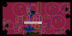
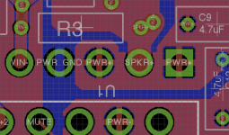
You can probably get the signal ground pour to flow through on the east side of R6 if you scoot the trace connecting R6 and C3 to the other side of the pad of HBR.
The OUT pour doesn't help you on the east side of the R5/C4 trace. I suggest using that area either for the power supply pour or scoot the 45º trace on the R5/C4 connection north to the end of R5. That will allow the OUT pour to be a bit wider.
It looks like you have a trace exiting north from Pin 3 of the LM3886 (OUT) which prevents the pour from filling in correctly.
You may also be able to get the pours to fill in a bit better by changing the trace width of the pour. Typically pours are formed by many traces in parallel. By making the trace width smaller, you can get the pour to get into tighter spots. Just make sure the width you use will work for your PCB manufacturer. I usually use something like 10 mil traces for the pour even if the manufacturer will go smaller.
Double-check your pour-to-pour clearances. VCC/VEE/OUT look tight under the IC. Make sure you have enough clearance to survive the voltage. Various calculators are available if you google "PCB trace spacing calculator voltage".
Just suggestions. Looks pretty decent otherwise. I've attached a screen shot with the three areas marked that I spoke to above.
Tom
Attachments
Last edited:
Thanks again. I've made all the changes you suggested - the 0.25mm / 10 mil trace width on the polygons worked a treat getting into all the tight spots but left me with weedy looking connections to the pads so I got rid of all the thermal reliefs on the top layer pours. Guess I'll try using a biggish solder tip and try to keep the dwell times down.
Attachments
It looks like C8 is turned ever so slightly CCW. Is that just an artifact of the screen shot rendering?
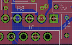
You have a little bit of a trouble spot around pins 3 and 5 of the LM3886. You can always go straight out of pin 3 with a fat trace (say 80 mil) into the pour. Getting into pin 5 is harder. I'd rejigger the pours such that you get at least two spokes on the thermal relief on pin 5 at the expense of the pour to pin 3. This will require you to set the grid spacing in the software a little tighter.
I definitely recommend using thermal reliefs when you're using planes. Just use a reasonable sized annulus and make sure the spokes can handle the current.
Curious question: What're the board dimensions currently?
Tom
Attachments
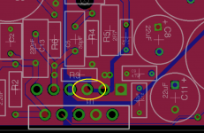
I was worried about that area, I think I'll try as you suggest and run a trace from pin 3. When I calculated the separation for the voltage (assuming 76V potential difference between +/- power planes) it was coming in at just short of 1mm about 38 mil. It's really difficult to get that separation between the pins and get decent contact area. I'll have a go at re-drawing those top planes.
The problem I'm getting with the thermal relief is that when I'm using a polygon trace width of 0.25mm the spokes come out at the same width - I tried drawing over the spokes with a wider trace but it came out a bit messy - I guess I just need to zoom in a bit.
The board's measuring 79mm x 39mm at the moment.
Last edited:
Is there no setting for the spoke width some place else? Like a global thermal relief setting somewhere? That's annoying. Are you using Eagle?
If you're just assembling a few boards for yourself, I wouldn't be overly concerned about the thermal reliefs. The connections to the pours will be annoying to solder and you might need a tip with some thermal mass to it, but it's doable. If the alternative is thermal relief spokes that turn into fuses, the solid pours are much preferred.
Tom
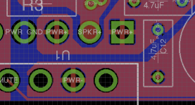
Here's the updated layout. I've managed to get four spokes to each of the power pins with the trace between pins 1 & 5 down to just under 1mm at the narrowest point. I couldn't decide whether to trade off the gap between VCC & VEE or get a wider trace between 1 & 5, so they're roughly equal. I might try a bit harder to get that pour to join up around the top-left of pin 1.
Thanks,
Simon.
Thanks,
Simon.
Attachments

Here's a close up, the grid is set to 0.5mm. I'm still worried about the width of the trace between 1 & 5 - on a previous version I had those pins connected with a trace on the bottom layer... seems a shame to interfere with that nice big ground plane though.
Simon.
Simon.
Attachments
Last edited:
My concern with letting Eagle do it's job was that it brings the VCC plane very close to the speaker pin. When I added an isloate value to the polygon the layout got worse.
I'm no expert with Eagle and perhaps I don't need to worry about the gap between VCC and pin 3.
Heres a pic of what it looks like with the pour going right across pin 3.
Thanks,
Simon.
I'm no expert with Eagle and perhaps I don't need to worry about the gap between VCC and pin 3.
Heres a pic of what it looks like with the pour going right across pin 3.
Thanks,
Simon.
Attachments
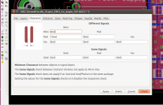
You have to properly configure clearances between various objects according to the max potential differences (see attached). Use this clearance calculator to get reliable numbers.
Thanks Oleg, if I use that calculator it gives me more wiggle room (0.13 mm spacing as opposed to 1mm) - does the resist layer on the pcb mean that I can use the 'coated' output?
Thanks,
Simon.
A hint - navigate to Tom's www.neurochrome.com web page, find "LM3886 Done Right" and look at how the Master did it")
A hint - navigate to Tom's www.neurochrome.com web page, find "LM3886 Done Right" and look at how the Master did it
Thanks, I can't remember how many times I've read those pages - I'm on a steep learning curve so I don't know how much I've really properly understood which is why this thread has been invaluable to me.
- Status
- This old topic is closed. If you want to reopen this topic, contact a moderator using the "Report Post" button.
- Home
- Amplifiers
- Chip Amps
- Newbie LM3886 Circuit