10mA through a V rated k170/j74 is no problem IF YOU KEEP A SENSIBLE LIMIT ON PD of each FET.
i.e. Vds must be low. Do you need to consider changing the voltage coming from a cascode?
Output currents affect the voltage drop over the BJT emitter resistors.
This in turn sets the FET currents. It is the FET currents that should be matched. But the schematic does not show appropriate resistors to do this setting up, hence the distortion adjustment.
It seems my explanation was not appreciated, you missed the message contained therein.
gk7 said:2nd try.
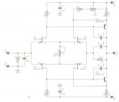
I have slightly increased the drain resistors and made the collector resistor of one BJT adjustable (12.5 - 32 Ohms) to adjust the output stage for equal currents through both BJTs.
Resistor brand: Vishay-Dale CMF-55-143 (good ? not good ?)
Currents: approx. 10mA for each FET (more ? less ?)
approx. 27mA for each BJT (they will dissipate 0.45W each, should be ok with small heatsinks).
Please comment, especially on the current through the FETs ...
I use a 1K trim pot to replace R2 or R3 to adjust the offset voltage at the output.
AndrewT said:10mA through a V rated k170/j74 is no problem IF YOU KEEP A SENSIBLE LIMIT ON PD of each FET.
i.e. Vds must be low. Do you need to consider changing the voltage coming from a cascode?
Output currents affect the voltage drop over the BJT emitter resistors.
This in turn sets the FET currents. It is the FET currents that should be matched. But the schematic does not show appropriate resistors to do this setting up, hence the distortion adjustment.
It seems my explanation was not appreciated, you missed the message contained therein.
Hi Andrew,
your input certainly was appreciated but I think your explanaition has some flaws.
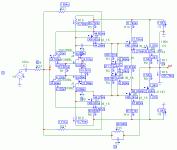
Let me explain how this circuit works:
The FETs are complementary differential pairs. One could feed them
by a current source for each pair connected to their sources to
set their current, like it is done in most other circuits of this type.
But because the sources of the upper FETs are
at a (small) positive and the lower ones at a (small) negative voltage,
a simple resistor will do. The value of this resistor sets the current
through it. This was first used by John Curl and is one
of the points that make this circuit so elegant.
This resistor is the pot R1 (50 Ohms) in my schematic. This is where
the current through the FETs is adjusted.
The current through the FETs defines the voltage across the drain resistors
(R1, R2). This voltage in conjunction with the emitter resistors of the
BJTs (R4, R5) sets the current through the output stage.
For 10mA through each FET and an estimated 0.6V base-emitter voltage for
the BJTs it would be approx. (10mA * 113 Ohm - 0.6V)/20 Ohm = 26.5 mA
The BJTs work like constant current sources to each other, this is why
this type of circuit is a transconductance amplifier (converts input voltage to output current).
If the two halves of the circuit are not perfectly identical (which is
likely because unfortunately no perfect complementary devices exist)
one could adjust the current through the output stages in two ways:
Adjust one drain resitor and thus the voltage the corresponding BJT sees
on it´s gate (this is what HKC did) or adjust the emitter resistor of
one BJT (like in my schematic).
more corrections / additions
The approximation for the current of the output stage is not
really exact. It would be ok if we would not have a folded
cascode. With the folded cascode the current for the right
device of of a FET pair goes through the emitter resistor too.
For low FET currents and high currents through the bipolars
the approximation would probably be close enough, but to
be close to the original circuit I would want relatively high
current for the FETs. Maybe I will have to increase the
drain resistors further (or the FET current to approx. 12mA)
to have enough current through the BJTs (25 mA per device).
Hi,
the 50r sets the total current through the FETs.
There is no way to check how much of that current goes either side of the FET LTPs.
If IMD = intermodulation distortion adjustment then it shows that the designer has recognised the need to balance the currents in the two halves of the LTP.
It also appears that having been aware that the currents needed to be balanced, he did not want to insert extra resistors in his circuit to enable monitoring of the effectiveness of the balance.
You seem to have completely missed this point.
AndrewT said:Hi,
the 50r sets the total current through the FETs.
There is no way to check how much of that current goes either side of the FET LTPs.
If IMD = intermodulation distortion adjustment then it shows that the designer has recognised the need to balance the currents in the two halves of the LTP.
It also appears that having been aware that the currents needed to be balanced, he did not want to insert extra resistors in his circuit to enable monitoring of the effectiveness of the balance.
You seem to have completely missed this point.
Do you refer to the same part numbers as I do ? I have attached the schematic again.
Yes the 50R pot (R1) sets the current through the complementary differential FETs, nothing else. If you don´t believe me, Erno Borbely has an excellent description of this circuit on his website you might want to read.
The "IM Balance" in the other circuit is a later addition of Tom Colangelo to John Curls original circuit. If "IM Balance" really means "IMD Adjustment" like you interpret it - I´m not sure. Certainly it adjust the current of one half of the BJT output stage not the current through the FETs. (Which is set by the current source located between their sources).
Attachments
I do believe you.
But, you are looking at the circuit from the wrong direction.
The voltage across R2= Q5Vbe+ V{r4//[r8+r9]}
The quiescent current in Q5 directly affects the quiescent currents in Q1 & Q2.
The ratio of R2 : r4//[r8+r9] affects the balance of currents in Q1 & Q2.
It is this balance that cannot be measured with the existing circuit. I think that's why the designer is using the IMD adjustment.
AndrewT said:I do believe you.
But, you are looking at the circuit from the wrong direction.
The voltage across R2= Q5Vbe+ V{r4//[r8+r9]}
The quiescent current in Q5 directly affects the quiescent currents in Q1 & Q2.
The ratio of R2 : r4//[r8+r9] affects the balance of currents in Q1 & Q2.
It is this balance that cannot be measured with the existing circuit. I think that's why the designer is using the IMD adjustment.
You mentioned an article (from D. Self I believe) where he describes how this would have an influence on intermodulation distortion.
Do you have a link to this article ?
BTW John Curl, who designed the original circuit, does not use that adjustment, but the line modules of my ML-1 (sealed in epoxy so we will never know for sure what is actually in them) have a second pot. I just guessed that it might have a similar purpose like in the ML-2 frontend (which is a John Curl design modified by Tom Colangelo).
Yor equation R2= Q5Vbe+ V{r4//[r8+r9]} is certainly correct, but I still believe that its the other way round: The quiescent current in Q1 directly affects the quiescent current in Q5. (The voltage through R2 is set by the current source of the LTPs and with both inputs of a differential amplifier at 0 V (no signal condition) the currents through both halves should be equal, no ?)
No.gk7 said:.......... and with both inputs of a differential amplifier at 0 V (no signal condition) the currents through both halves should be equal, no ?)
You have to adjust to make them equal.
AndrewT said:
No.
You have to adjust to make them equal.
Actually no. It´s a differential (!) amplifier. Equal input = equal output
JFET differential pair with true differential input and true differential output: It sees voltage difference at the input and current difference at the output.
In static condition (no signal) we have zero voltage difference at the inputs and thus zero current difference at the outputs.
In static condition (no signal) we have zero voltage difference at the inputs and thus zero current difference at the outputs.
now add your cascode.
What are the currents flowing in the three semis?
The rule for an opamp (differential amplifier) is that the feedback tries to ensure that the difference across the inputs is near zero. That can and will be achieved even when the input LTP has different currents in the two halves.
What are the currents flowing in the three semis?
The rule for an opamp (differential amplifier) is that the feedback tries to ensure that the difference across the inputs is near zero. That can and will be achieved even when the input LTP has different currents in the two halves.
AndrewT said:now add your cascode.
What are the currents flowing in the three semis?
The rule for an opamp (differential amplifier) is that the feedback tries to ensure that the difference across the inputs is near zero. That can and will be achieved even when the input LTP has different currents in the two halves.
With no signal there is no difference on the inputs. It seems it is not easy to convince you, but there was a thread about building the JC-3 which uses this topology for the voltage amplifier. I don´t find the link but I have attached a simulation from this thread, I have saved. There you have 44.3 mA through each BJT and 6.1 mA through each (!) FET.
Attachments
original link to thread
http://www.diyaudio.com/forums/attachment.php?s=&postid=1291734&stamp=1188624090
The simulation was made by PMA (Pavel Macura) who is a member here.
http://www.diyaudio.com/forums/attachment.php?s=&postid=1291734&stamp=1188624090
The simulation was made by PMA (Pavel Macura) who is a member here.
look at the ratio of currents in R18 & R5. ~8.75:1
now change either R18 or R5 slightly (equivalent to trimming/adjusting the collector resistor).
What effect does this have on the FET currents, if any? with whatever R18 & R5 are in the posted schematic the imbalance between Q1 & Q4 is <0.09% and J2 & J3 is <0.05%. I can't ask anyone (or any circuit) to do better than that.
If one does not trim the collector resistor values, what happens?
AndrewT said:look at the ratio of currents in R18 & R5. ~8.75:1
now change either R18 or R5 slightly (equivalent to trimming/adjusting the collector resistor).
What effect does this have on the FET currents, if any? with whatever R18 & R5 are in the posted schematic the imbalance between Q1 & Q4 is <0.09% and J2 & J3 is <0.05%. I can't ask anyone (or any circuit) to do better than that.
If one does not trim the collector resistor values, what happens?
"change either R18 or R5 slightly (equivalent to trimming/adjusting the collector resistor)" - this is plain wrong, R18 is the drain resistor.
"What effect does this have on the FET currents, if any?" - none, their currents are set by R1.
This leads to nothing, me thinks ... The simulation should be clear, I believe...
- Home
- Source & Line
- Analog Line Level
- Need to build JC 2 preamp