Agreed. Provided we select the right polarity of an electrolytic cap to suit the DC potential difference between TR2 base and ground, we can use any standard electrolytic cap for the FB cap. Note that the polarity shown on the schematic will likely be wrong so measure and prove it for yourself.
Naim just happened to like the idea of TAG tantalum caps because they were cool and new to audio, 45 years ago when the product was developed. You'll find standard, 100uF 16-25V electrolytics will fit most clone PCBs and you can also use non-polarised and special audio types if you wish but any benefit would likely be insignificant there.
Naim just happened to like the idea of TAG tantalum caps because they were cool and new to audio, 45 years ago when the product was developed. You'll find standard, 100uF 16-25V electrolytics will fit most clone PCBs and you can also use non-polarised and special audio types if you wish but any benefit would likely be insignificant there.
Attachments
Rensli I have a box of FB caps std 100uf electros 100uf bp 50uf bp all makes etc along with bead taints wet dry brass case etc but not sure why but the Axial Tantalum Capacitors Vishay-Sprague, i will look at ian comment Note that the polarity mmm me thinks could be right my off set is down to 0 mv on my test rig however the rest 24 in all are 20>50mv off set
i will look at ian comment Note that the polarity mmm me thinks could be right my off set is down to 0 mv on my test rig however the rest 24 in all are 20>50mv off set
Just to remind you guys, as written many times before for people who read old posts, the offset of this amp can be easily tuned to 0mV by playing with the total input resistance vs the feedback resistance. It's simple as that. It's not dependant on the LTP transistors beta, LTP balance and so on ... or if it is, the effect is really, really minimal.
My clones were at around 5-7mV... Not that it matters for the sound quality...
Last edited:
Perhaps we are talking about different issues but the voltage at TR1,2 bases is not necessarily the same as that at the output. Dave S has commented on this in recent times regarding his NC200 clone. He states that quasi-comp designs will have a negative potential at both LTP bases due to the assymmetry of the output stage, hence a reversed polarity may be needed for both caps. That comment probably originated at Avondale Audio but Traderbam recently repeated it, in reference to the attached schema.
I haven't noticed it as being significant and a quick check of a standard LJM clone board I have, shows that there is a difference but not more than 100mV which tracks with any DC offset at the output.
Having just now checked the voltage difference on a finished Ebay clone, the small negative base potential is there, but only about 100mV different to the output DC voltage - not a big concern.
Attachments
LTP base voltage
Imagine the amplifier being perfectly adjusted so that the output dc offset is zero. Assume the LTP transistors are identical and each have, for instance, a beta of 250.
The Ie of each transistor will be the LTP CCS divided by 2 or, say, 500uA. This means the base currents will each be 500uA/250 = 2uA. This current has to flow somewhere and it flows through the dc resistive paths to 0V. On the non-inverting base this will be via 4.7k and 22k in series, a total of 26.7k. On the inverting base it will be through 27k to the output, which is at 0V. The voltage drop across 27k caused by 2uA is 54mV. So when the system is fully matched and adjusted, you would expect each base to be about 54mV negative with respect to 0V.
Note that in a low or no NFB design the LTP differential voltage can get larger than the dc offset voltage and can go above 0V and cause your dc blocking capacitors to see a reverse voltage. In this case use non-polarized capacitors. This can also happen in a high NFB design if you haven't set it up properly or a fault occurs...so to be on the safe side while perfecting your design, don't use tantalums.
PS: the same advice if you are using JFET or MOSFET transistors in your LTP. They have virtually zero gate current so the gates will swing above and below 0V.
LTP base voltage
Imagine the amplifier being perfectly adjusted so that the output dc offset is zero. Assume the LTP transistors are identical and each have, for instance, a beta of 250.
The Ie of each transistor will be the LTP CCS divided by 2 or, say, 500uA. This means the base currents will each be 500uA/250 = 2uA. This current has to flow somewhere and it flows through the dc resistive paths to 0V. On the non-inverting base this will be via 4.7k and 22k in series, a total of 26.7k. On the inverting base it will be through 27k to the output, which is at 0V. The voltage drop across 27k caused by 2uA is 54mV. So when the system is fully matched and adjusted, you would expect each base to be about 54mV negative with respect to 0V.
Note that in a low or no NFB design the LTP differential voltage can get larger than the dc offset voltage and can go above 0V and cause your dc blocking capacitors to see a reverse voltage. In this case use non-polarized capacitors. This can also happen in a high NFB design if you haven't set it up properly or a fault occurs...so to be on the safe side while perfecting your design, don't use tantalums.
PS: the same advice if you are using JFET or MOSFET transistors in your LTP. They have virtually zero gate current so the gates will swing above and below 0V.

In my experience the Naim circuit, due to small leakage here and there, the 26.7k vs 27k, plus second transistor of the LTP with slightly higher beta, will always give negative DC offset. At least, that's what I've measured.
I guess they were pretty sure of the consistency of the offset and used tantalums without troubles.
When using polar electrolytics we are told they generally tolerate reverse voltages up to around 1Vpk to 1.5Vpk.
The ensure a polar electolytic can survive a short term reverse voltage one fits a signal diode across it to pass the current coming in through the NFB from a railed output.
I don't think a Tantalum can accept any reverse voltage. I can't recall seeing any advice for acceptable short term reverse voltage.
Andrew have a look at this page 6
http://www.vishay.com/docs/40110/faq.pdf
http://www.vishay.com/docs/40110/faq.pdf
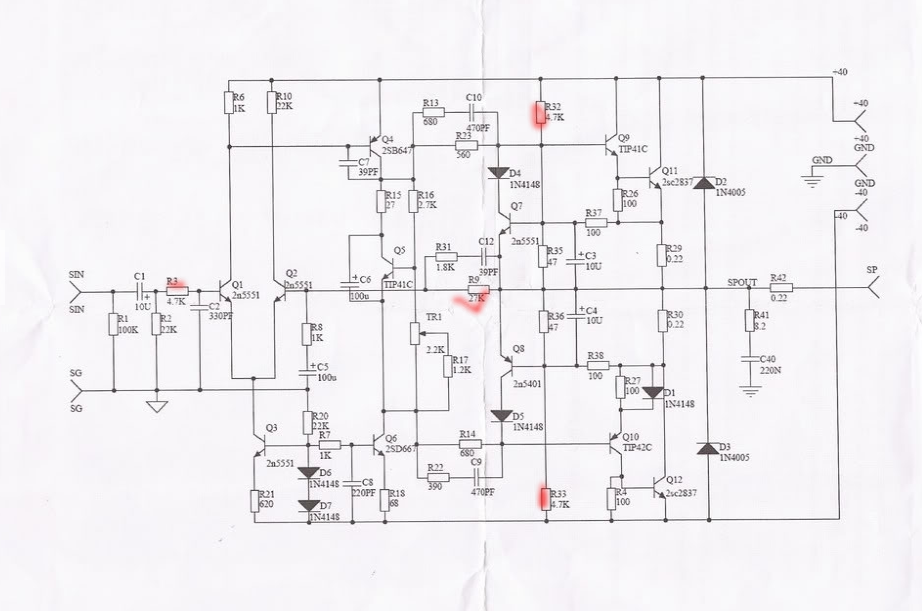
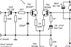
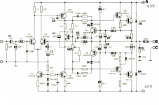
R13/23 and R14/22 are part of those small RC networks which correct phase differences at high frequency but some other models don't fit the networks at all. It's not critical that you use the exact values there but 27/33R seems quite wrong. Where did those values originate? For reference, look at the NAP schematic, shown several times in this thread, rather than the kit supplier's, though importantly, that will show their adjusted values to suit the range of parts supplied in their kits.
Note also that the specified 40V supply voltages are actually for NAP250. Don't exceed those rail voltages on any variation using the original semis. The semis supplied with cheap kits are rated at higher voltages but don't have enough heat dissipation anyway. In the real products, models such as NAP 140 use lower rail voltages and some resistor values are also slightly reduced to provide consistent bias currents in the front end. Otherwise, the same schematic is suitable for all early NAP models.
BTW, Q5, the Vbe multiplier transistor - TIP41? Amazing, I wonder what they were thinking when any small NPN will do fine there. If it needs to be attached to something, a BD139 or 2SD669 would be OK, otherwise any TO92 like BC548, 2N5551 etc can be used.
Attachments
there but 27/33R seems quite wrong. Where did those values originate?
Hi, if i get time today, i will point you to the values presented here.
27R/33R has been common on NAP140 circuit, were non-regulated and small VA transformer, smaller values usually are used on upper NPN DRIVER BASE.
I have myself played with these filters and know, if filter network resistor values are high, the sound becomes more dry and potential of oscillation will rise.
If lower values are used, there is less chance for oscillation, sound profile also changes.
Most interesting part i experienced, is that if you loop one middle octave piano note and listen very closely to a speaker while turning trimpots on filter networks...you can actually hear some effect/noise with the piano note coming out and fading away, depends on resistor values
Hmm... that effect seems like drive current starvation.
When I simulate a generic amp (that's a Naim without the tweaks - same as that discussed at length in Douglas Self's articles and books) I find lowest THD with around 30R driver base stoppers. Traditional, nominal values have been 100R in many model designs I've seen and built but confess that I haven't played much with those values. There's a lot of fans of those early Naits but I wonder whether that has more to do with affordability than outright SQ.
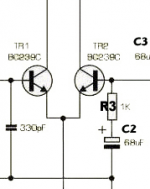
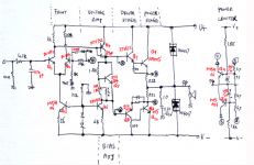
If you look at Nait models 1 and 2 at least, (attached is a hand sketched circuit from the net) you can see that the RC network is just omitted and not a stopper resistor is in sight - the VAS will die too when an output device shorts.
When I simulate a generic amp (that's a Naim without the tweaks - same as that discussed at length in Douglas Self's articles and books) I find lowest THD with around 30R driver base stoppers. Traditional, nominal values have been 100R in many model designs I've seen and built but confess that I haven't played much with those values. There's a lot of fans of those early Naits but I wonder whether that has more to do with affordability than outright SQ.
If you look at Nait models 1 and 2 at least, (attached is a hand sketched circuit from the net) you can see that the RC network is just omitted and not a stopper resistor is in sight - the VAS will die too when an output device shorts.
Attachments
1.
The 27/33R are at the green PCB:
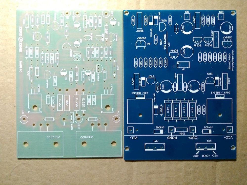
I't not a kit. Only PCB. (C2240 ) (http://www.diyaudio.com/forums/solid-state/112453-nap-140-clone-amp-kit-ebay-251.html#post5024464)
2. Q5 is C2240
It's not critical that you use the exact values there but 27/33R seems quite wrong. Where did those values originate?
The 27/33R are at the green PCB:
I't not a kit. Only PCB. (C2240 ) (http://www.diyaudio.com/forums/solid-state/112453-nap-140-clone-amp-kit-ebay-251.html#post5024464)
2. Q5 is C2240
Ah, thanks Alex74, I have a pair of those on order as full kits but didn't realize they incorporated such a modification. Strange days when clone kit suppliers just follow their own path but use the same titles as the correct circuit, but with another different schematic that doesn't match either boards 
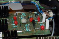
There are countless photos about these resistor values, al seems legitable and original.
http://www.hifishock.org/galleries/electronics/naim/power-amplifier/nap-140-2-naim.jpg
naim power amplifier nap 140 3 naim - Hifi audio
naim power amplifier nap 140 4 naim - Hifi audio
http://www.hifishock.org/galleries/electronics/naim/power-amplifier/nap-140-2-naim.jpg
naim power amplifier nap 140 3 naim - Hifi audio
naim power amplifier nap 140 4 naim - Hifi audio
Attachments
- Home
- Amplifiers
- Solid State
- NAP-140 Clone Amp Kit on eBay