What's Next
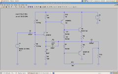
Here is some more tinkering with the design, performance has gotten a lot better, but the real world transistors in the sim would need to be replaced with something comparable that can dissipate the required power. The output stage is biased to something like 380mA quiescent (a little into class AB at 1Wrms level) which would fry the devices in the simulations. The nice or not so nice thing about spice is that it will allow you to run devices without regard to their voltage, current or dissipation ratings. Good working simulated circuits that would blow in the real world are quite possible. Generally similar devices with the required power handling are available. The jfet is fine as is for the supply voltage shown. Lower impedance loads probably not a good idea..
Note that the comment about dissipation could be true for the other simulations as well.
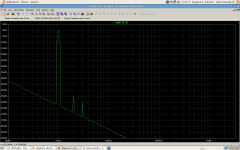
The FFT is at 1Wrms output... Note that the dominant harmonic is now 2nd, third is even further down, and higher order are not significant. Who knows this might even sound good with careful selection of appropriate devices and some addition work to optimize operating points for the devices chosen. As a tube guy I'm not going down this path for the moment, but hmmm I might think about it for the future.
Edit: Some further details from the simulation:
1. Q2 collector current is 64mA.
2. Output stage quiescent current is 380mA.
3. Output stage is symmetrical at half supply.
4. Open loop gain has fallen to approximately 41dB.
Linearity in the VAS has improved significantly, and greatly in the output stage, hence the improved sims.
Here is some more tinkering with the design, performance has gotten a lot better, but the real world transistors in the sim would need to be replaced with something comparable that can dissipate the required power. The output stage is biased to something like 380mA quiescent (a little into class AB at 1Wrms level) which would fry the devices in the simulations. The nice or not so nice thing about spice is that it will allow you to run devices without regard to their voltage, current or dissipation ratings. Good working simulated circuits that would blow in the real world are quite possible. Generally similar devices with the required power handling are available. The jfet is fine as is for the supply voltage shown. Lower impedance loads probably not a good idea..
Note that the comment about dissipation could be true for the other simulations as well.
The FFT is at 1Wrms output... Note that the dominant harmonic is now 2nd, third is even further down, and higher order are not significant. Who knows this might even sound good with careful selection of appropriate devices and some addition work to optimize operating points for the devices chosen. As a tube guy I'm not going down this path for the moment, but hmmm I might think about it for the future.
Edit: Some further details from the simulation:
1. Q2 collector current is 64mA.
2. Output stage quiescent current is 380mA.
3. Output stage is symmetrical at half supply.
4. Open loop gain has fallen to approximately 41dB.
Linearity in the VAS has improved significantly, and greatly in the output stage, hence the improved sims.
Attachments
Last edited:
in my simulations of a closely related circuit,, distorsion is no more than 0.02 %,
even at 10 khz, for a 22V pp output...
the tirany of the dc coupled fashion make these amps
irrelevant, even they perform as well as the dfferential based ones..
the output capacitor is the warranty that the speakers will
survive whatever happen to the thing..
even at 10 khz, for a 22V pp output...
the tirany of the dc coupled fashion make these amps
irrelevant, even they perform as well as the dfferential based ones..
the output capacitor is the warranty that the speakers will
survive whatever happen to the thing..
Edit: Some further details from the simulation:
1. Q2 collector current is 64mA.
2. Output stage quiescent current is 380mA.
3. Output stage is symmetrical at half supply.
4. Open loop gain has fallen to approximately 41dB.
Linearity in the VAS has improved significantly, and greatly in the output stage, hence the improved sims.
Noted that more than half of J1 drain current is flowing through the base of Q2, further simulation revealed that a reduction of 2nd harmonic of about 6dB was possible by increasing R1 to 20K which slightly increases the open loop gain and results in most of the drain current flowing through the base of Q2. Perhaps not what we would consider a great design practice...
 This all hangs quite precariously on the characteristics of the transistors used - quite a departure from what today would be considered good design practice.
How well this would work in practice is another question.
One further suggestion I have if anyone is actually thinking about building any variant of this design is the replace the bootstrap with a simple CCS - the current flowing through the load particularly in my "improved" version is far too high for a quality loudspeaker, depending on VC dcr the standing dc voltage across the voice coil could be in the vicinity of 400mV - not a very good idea.
wahab,
Agreed.getting rid of htis antic kind of bootstrap is the first thing to do,
and replace it as you say by a current source...
Not generally true.second is to use a pair of darlingtons as output stage..
the results will be well better..
Could you elaborate on that?the tirany of the dc coupled fashion make these amps
irrelevant, even they perform as well as the dfferential based ones..
Yet Another Variant
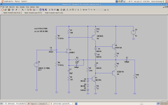
Here is the latest with a sleazy CCS substituted for the original boot-strap. FFT shows similar preponderance of 2nd - 3rd order distortion in the spectra. It is a couple of dB higher however. The output power is 1Wrms.
Using a darlington output stage would introduce an additional pole inside of the loop making it harder to compensate, and IMO isn't necessary for a very low power amplifier design such as this..
Obviously some additional work would be required to compensate this amplifier with the appropriate transistors. The CCS and 2nd VAS transistor should be able to dissipate a couple of watts each, and the output transistors should handle a couple of amps and be able to dissipate 30W or so each..
Compared to more modern designs this one has quite limited open loop gain and the feedback margin is slightly under 20dB (10X). It might be worth building for a small efficient full range speaker system.. The quality of the output capacitor is important. The design has no zobel network on the output, nor a series inductor - I leave it to others to determine whether or not these are needed in a specific application.
Attachments
Last edited:
wahab,
Not generally true.
Could you elaborate on that?
lumba,in that case, it s true, as a single output pair
doesn t provide high gain, all it does is to crush
the vas gain, the impedance of the final stage being very low..
a better way would be to use hitachi s 162/1058..
as you know, modern amps are required to have a
dc coupled output..
the capacitive coupled output amps are considered
out of date, at least in a marketable point of view...
Kevin,
you did a great job. JFETs should not be forward-biased.
It's a curious design..
Depending on the fet chosen the bias will be approximately -2V from gate to drain, so technically it isn't forward biased if I understand your comment. (The FET operating point actually makes the output stage center at about 1/2 the supply rail - at least in the simulations, some tinkering might be required in real life to get it close.) Actually this bias arrangement is a very common approach in musical instrument fet front ends and works fine with a little care.wahab,
some topologies provide far greater advantage that the deterioration caused by an electrolytic capacitor.
yes, and this particular cfb topology is
extremely good, even with few components..
wahab,
Much better than that you were showing me anyway...yes, and this particular cfb topology is
extremely good, even with few components..
Thank you for all your contributions; I didn't expect quite such an interest and it's very nice that so many people are trying to help.
I'm considering building a version of the amp just to see how it performs, albeit with some modifications:
(a) the output stage biased to class A (obviously not with the original transistors but some beefier devices on a suitable heatsink) and
(b) closed loop gain reduced to about 20 dB.
My experience with this particular architecture that it sounds better than one would expect from the measurement/simulation results. A few years ago somebody I know spent quite a bit of time experimenting with different architectures and said that - in his subjective opinion - amplifiers with this type of input stage (where the feedback from the output is connected to the emitter/source of the first transistor with the input on the base/gate) sound better than ones with a long tail pair on the input. Also, he reckoned that replacing the "capacitive booster" on the driver stage with a constant current source made no improvement in sound quality even though simulation and measurement showed much improved linearity. However, again, this was just his subjective opinion.
With regard to the 4.7K in the drain of the FET, I am still a bit unsure about its function but hey-ho, I can live with it.
(Also, I hope the rabbit is OK, incidentally I have a rabbit too and a few years ago we lost one due to illness so I know how upsetting it can be.)
MajorMajor,
Please read John`s post #27 then forget about that resistor.With regard to the 4.7K in the drain of the FET, I am still a bit unsure about its function but hey-ho, I can live with it.
Andrew,
It indicates a completely improper Q-current.I'm pretty sure I read that .6 volts was found across that resistor. That would make it a pretty poor dissipation limiter for T1.
wahab,
Much better than that you were showing me anyway...
you like joking , lumba...
although excellent, it can t compare to a simple differential
amp well designed, let alone a symetrical differential one...
- Status
- This old topic is closed. If you want to reopen this topic, contact a moderator using the "Report Post" button.
- Home
- Amplifiers
- Solid State
- Mystery resistor in simple audio amp