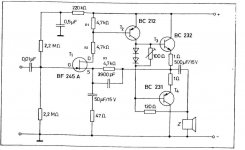
Thanks for your suggestions. Let's for a second leave aside the possibility that the 4.7K resistor was only included to confuse the Russians; somehow I do not believe a rouge resistor in an audio design would have dealt a major blow to the might of the Soviet military forces...
It is also clear that the resistor has negligible effect on the steady state AC and DC conditions. Simulation shows that its effect on the open loop gain is less than 1%. So we are left with the possibility that it has some secondary (RF suppression) or transient protection function.
I tend to favour the argument that it is for transient protection but I still can't see why it's needed. Let's suppose the resistor it's not there (i.e. shorted out). OK, at the moment of power-up, the 47uF cap is short circuit, so the FET source will be connected to ground through a 47 Ohm resistor. Now the Idss (saturation drain current) of the BF245A is specified as 6.5 mA maximum, which for a very-very short time may occur (although it would immediately cause the source to go positive due to the voltage drop on the 47 Ohm resistor in the source, so I would expect even this 6.5 mA only to last a few nsec) but then - so what? The 6.5 mA current is far too small to cause any damage to the BC212 base-emitter junction and the FET can also handle 50 mA maximum drain current. Even at 6.5 mA and the maximum 24V supply voltage the FET dissipation is only about 150 mW - again, no problem, it can handle 360 mW continuously (and, as before, these are absolute maximum worst case transient figures). So, unless I have overlooked something, even under worst-case transient conditions all devices are operated well within limits that they are specified to handle continuously!
When it comes to the other possibility, RF suppression, again, somehow it doesn't make sense. In my experience, the BF245 series is really not very prone to this anyway and even then it's usually fixed by the usual gate-stopper resistor.
Finally, this is definitely not just a design on paper, the book shows some measurement results for quiescent current, distortion, etc, so clearly the circuit was built and tested.
Arhh, it's so frustrating because the design is so simple... Could somebody please locate the original design engineer and interrogate him...") ?
?
It is also clear that the resistor has negligible effect on the steady state AC and DC conditions. Simulation shows that its effect on the open loop gain is less than 1%. So we are left with the possibility that it has some secondary (RF suppression) or transient protection function.
I tend to favour the argument that it is for transient protection but I still can't see why it's needed. Let's suppose the resistor it's not there (i.e. shorted out). OK, at the moment of power-up, the 47uF cap is short circuit, so the FET source will be connected to ground through a 47 Ohm resistor. Now the Idss (saturation drain current) of the BF245A is specified as 6.5 mA maximum, which for a very-very short time may occur (although it would immediately cause the source to go positive due to the voltage drop on the 47 Ohm resistor in the source, so I would expect even this 6.5 mA only to last a few nsec) but then - so what? The 6.5 mA current is far too small to cause any damage to the BC212 base-emitter junction and the FET can also handle 50 mA maximum drain current. Even at 6.5 mA and the maximum 24V supply voltage the FET dissipation is only about 150 mW - again, no problem, it can handle 360 mW continuously (and, as before, these are absolute maximum worst case transient figures). So, unless I have overlooked something, even under worst-case transient conditions all devices are operated well within limits that they are specified to handle continuously!
When it comes to the other possibility, RF suppression, again, somehow it doesn't make sense. In my experience, the BF245 series is really not very prone to this anyway and even then it's usually fixed by the usual gate-stopper resistor.
Finally, this is definitely not just a design on paper, the book shows some measurement results for quiescent current, distortion, etc, so clearly the circuit was built and tested.
Arhh, it's so frustrating because the design is so simple... Could somebody please locate the original design engineer and interrogate him...
?The drain impedance may not be low enough for an added 4.7k to cause a dramatic shift in response above the audio band, but it is cheaper than adding a capacitor from collector to base on T2. Barely enough would have been excellent in such a circuit that may have actually wound up in someone's hybrid tube-semiconductor TV audio output at the time.
I don't see how. R1 is paralleled by the low Rbe of T2. It looks to me like it's just there to set DC conditions of T2, which is a current source. R2 looks like it limits the base current of T2.
Really depends on the base resistance of T2 , but R1/R2 does form a voltage divider between the drain of the fet T1 and the supply rail. Depending on that transistor the attenuation between the drain of T1 and base of that T2 might be a lot more than 6dB.
T2 is the second stage of the VAS, it's not a current source at all, and notice how its collector load is boot-strapped to the load side of the output. (That 120 resistor effectively takes the place of a current source.)
I designed amplifiers like this as a kid, using a bi-polar in the input stage, they actually work and sound much better than you would expect. Early HH Scott transistor amps and receivers also used a very similar topology and you guessed it - sounded better than you would expect, and a lot better than what subsequently followed in the consumer sphere.
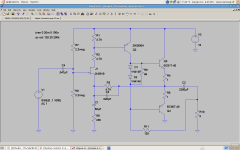
I've reposted the schematic in the interest of clarity. And I will probably simulate this circuit in LTSpice soon.
Attachments
Last edited:
I dunno, it looks to me like a CCS of I = 0.7/4k7, which then causes the voltage across the two diodes to be constant (the Vas). The bootstrapping, as far as T2 is concerned, doesn't really change the current (except for Early effect). Base resistance is low because T2 isn't degenerated. What am I missing?
Really depends on the base resistance of T2 , but R1/R2 does form a voltage divider between the drain of the fet T1 and the supply rail. Depending on that transistor the attenuation between the drain of T1 and base of that T2 might be a lot more than 6dB.
T2 is the second stage of the VAS, it's not a current source at all, and notice how its collector load is boot-strapped to the load side of the output. (That 120 resistor effectively takes the place of a current source.)
I designed amplifiers like this as a kid, using a bi-polar in the input stage, they actually work and sound much better than you would expect. Early HH Scott transistor amps and receivers also used a very similar topology and you guessed it - sounded better than you would expect, and a lot better than what subsequently followed in the consumer sphere.
I've reposted the schematic in the interest of clarity. And I will probably simulate this circuit in LTSpice soon.
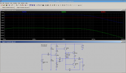
I have created a working simulation but have to go out on an urgent errand to pick up pet medications. (Sick bunny) However my contention that R1/R2 has an effect on loop gain is clearly shown in the SIM, and it isn't too subtle either. (10dB or so with transistors chosen)
I have created a working simulation but have to go out on an urgent errand to pick up pet medications. (Sick bunny)
Is that a euphemism?
Thanks for doing the sim. I'm interested to see it!
I have created a working simulation but have to go out on an urgent errand to pick up pet medications. (Sick bunny)
Is that a euphemism?
Thanks for doing the sim. I'm interested to see it!
OT: No, unfortunately, one of our rabbits has just started showing symptoms of e-cuniculi which killed his mate last summer. More here: Encephalitozoon Cuniculi Watching a loved pet going through this is absolutely heart wrenching.
I dunno, it looks to me like a CCS of I = 0.7/4k7, which then causes the voltage across the two diodes to be constant (the Vas). The bootstrapping, as far as T2 is concerned, doesn't really change the current (except for Early effect). Base resistance is low because T2 isn't degenerated. What am I missing?
That it's not a current source, but a common emitter amplifier.
The base current is actually proportional to some % of the drain current. The device operates as boot-strapped common emitter amplifier - the ac current in the collector circuit is reasonably constant, the dc current is controlled indirectly via the feedback loop. (Basically whatever current is required through the 120 ohm resistor to keep the output stage centered roughly at half supply.)
Last edited:
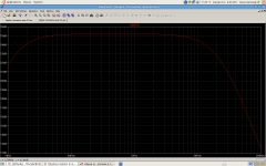
Here is the first screen shot which clearly shows the gain in the first stage is roughly 8dB (blue trace) and the signal present on the base of Q2 is 33dB lower (Green Trace) The red trace is the 0dB reference or input signal, all traces shown are relative to this value. What this means is the base resistance is actually extremely low and very little of the signal current actually flows through R1.
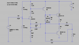
Note that I used typical transistors which are present by default in LTSpice IV, I haven't the inclination to add more suitable models, but this will illustrate the point.
I have posted a zip file of the LTSpice circuit model file - if you are an LTSpice user you can unzip and load this file right into LTSpice and run it, play with it to your heart's content.
That said the design has a gain closed loop gain of over 40dB, probably will not operate well on voltages higher than 15 - 20V without significant changes and appears to be designed to provide really high input impedance. The linearity is not that great. I will post an FFT at a couple of watts out - note that the output transistors are 500mA types because they were the most appropriate types, and have low beta. (25) I'll try higher beta versions as well and note the difference.
Attachments
Last edited:
Sorry to hear about your pet's illness. That was a very interesting article, though, thanks for the link.
The sim is indeed interesting.
Much appreciated.
The 70's, that was right in the middle of the Cold War. It was a practice to introduce strange technical items that had no purpose but would tie-up the other guys scientists for years trying to figure it out.
Keep trying to figure it out guys !
Seem a very poor technique for messing up any scientist
In my opinion is just a resistor that aid in preventing drain-gate breakdown (even partially, with device that become unusually noisy). In my experience jfet BF245 are not too rugged devices from this viewpoint: although their voltage limits are quoted as being 30 Volt, sometimes I've seen it starting to break just little above 20 Volt.
Hi
Piercarlo
A curiosity - no one mentioned the 120 ohm resistor between the base of t4 and the hot side of the load. Kind of a bootstrap circuit, but why send your voltage gain current through the load, unless some kind of bias for the load was desired? My guess is that this circuit was a drawn but not tested. Has anyone tried to simulate it?
This kind of bootstrap was quite common in these simple circuits. The reason of the trick was just for economising a second relatively bulk capacitor, using, for bootstrapping, the same yet used for output.
Hi
Piercarlo
This kind of bootstrap was quite common in these simple circuits. The reason of the trick was just for economising a second relatively bulk capacitor, using, for bootstrapping, the same yet used for output.
Hi
Piercarlo
Quite correct. This was a common technique to save the cost of a largish capacitor. The collector current in Q2 is relatively modest and so would not have presented a major issue for the loudspeaker on the output.
The resistors R1 and R2 play quite a large role in setting the amplifier's open loop gain as you can see if you take a look at my sims. (They are not there by accident.) I don't think R1 value is terribly critical so as long as the base resistance is several orders of magnitude lofower than it is. I am going to select a some transistors with higher betas..
The original amplifier was in the TI application book, I think the OP has replaced TI types with similar European numbers as TI would not have been selling competitors types!
Edit: In further syms it appears that there is not enough loop gain to properly close the loop - this may be a function of the transistors I selected, but I set input conditions for 1Wrms out and calculated the peak value required at the input to achieve this level and the output is a couple of dB low. Selecting amongst the few PNP types available to me has no effect, changing fets demonstrates that there are a fairly narrow range of jfets with relatively modest transconductances with which the circuit will work.
Last edited:
The resistors R1 and R2 play quite a large role in setting the amplifier's open loop gain as you can see if you take a look at my sims. (They are not there by accident.) I don't think R1 value is terribly critical so as long as the base resistance is several orders of magnitude lower than it is.
I'm not too sure about open loop gain magnitude but a role may be surely in play about open loop gain/frequency curve shaping. In some schematic i've yet seen this kind of added resistor with the goal of enhancing the local gain of some device and hence take advantage of Miller effect on its stray capacitances for lowering its roll-off frequency. I don't know if also this is a similar case. Maybe however, although I'm again quite convinced of some "breakdown braking" function (especially during circuit startup) related with R2. The two thing however surely don't cancel each other
Hi
Piercarlo
Current implementation has an open loop gain of just 45.2dB according to syms, which explains the unexpected results with a closed loop gain of 40.1dB..
The 2N3819 seems like the most appropriate choice for a jfet in the models I have, and the 2N2905 provides about the best performance again of the models on hand.
The current closed loop gain actually seems way too high so I will try setting it to a saner 26 dB and sim that.
The 2N3819 seems like the most appropriate choice for a jfet in the models I have, and the 2N2905 provides about the best performance again of the models on hand.
The current closed loop gain actually seems way too high so I will try setting it to a saner 26 dB and sim that.
Some fun with simple audio amp
I am coming to realize that this design was originally intended for some sort of relatively low end application, however it can be made to behave a bit better for a few watts out.. Why I am doing this I am not sure..
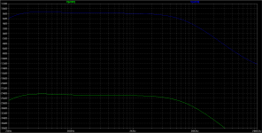
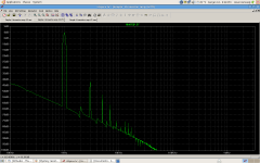
I have added an FFT of the modified circuit at approximately 1Wrms out, distortion is predominantly odd order and better than I expected for such a simple circuit, but I bet it doesn't sound real good..
I am coming to realize that this design was originally intended for some sort of relatively low end application, however it can be made to behave a bit better for a few watts out.. Why I am doing this I am not sure..
I have added an FFT of the modified circuit at approximately 1Wrms out, distortion is predominantly odd order and better than I expected for such a simple circuit, but I bet it doesn't sound real good..
Attachments
Last edited:
this schematic was common 35 yeras ago..
i did build one at the time, using a bjt at the input..
the schematic was on a motoroa ap note..
and as pointed in this thread, the sound is really
surprisingly good, at least in the bjt input i tested,
as it has at least 20 db OL gain more than the fet version..
an interessant explanation of this design can be found here
Simple 60 Watt Power Amplifier
this schematic was common 35 yeras ago..
i did build one at the time, using a bjt at the input..
the schematic was on a motoroa ap note..
and as pointed in this thread, the sound is really
surprisingly good, at least in the bjt input i tested,
as it has at least 20 db OL gain more than the fet version..
an interessant explanation of this design can be found here
Simple 60 Watt Power Amplifier
Me too... The loop gain can probably be increased somewhat..
- Status
- This old topic is closed. If you want to reopen this topic, contact a moderator using the "Report Post" button.
- Home
- Amplifiers
- Solid State
- Mystery resistor in simple audio amp