Either you did grow up next to the lead smelter or you really are just a gadfly.


I’m having limited time here to export my CAD package files, so I’ll just do a few quick and dirty screen grabs from my sim files, which pretty much represent the final circuit under construction anyhow.
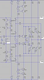
Figure 1 is a detailed diagram of the VAS, the VAS buffer and the bootstrapped voltage clamp.
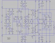
Figure 2 is just a zoomed out screen shot for a topological overview of the (almost) entire amplifier front end. Yes, the circuit is extravagant, but anyone who thinks that it looks complicated just hasn’t seen my +/-90V Vout linear series pass regulator for the (triple EF) power output stage yet.
The diamond buffer is biased by an LM336 2.5V voltage reference. Consequently the (bootstrapped) diamond buffer input transistors run at a healthy Vce of about 3V. To minimised VAS loading, these can be low voltage, high beta types. I’m using BC550C and BC560C in the prototype build.
The bootstrapped isolation diodes (D1 and D3) for the VAS voltage clamp are returned to the opposite terminals of the diamond buffer biasing voltage source. This achieves the operating reverse bias (of ~1.25V) that I mentioned in the last post.
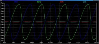
Figure 3 shows just how effective the bootstrapped clamp is. Figure 3 shows the diode currents with the output swinging 160V peak-to-peak, with the diamond buffer driving the 8k feedback resistance.
The red and cyan traces show the current through the bootstrapped isolation diodes, D1 and D3, which are connected to the VAS collector. The green and blue traces, on the other hand, show the current through the actual clamp diodes D2 and D4, which are subject to the full signal swing.
This is the current that would otherwise be loading the VAS, if not for the bootstrapping, or “flying clamp” operation.
At the end of the day I know that this is “just a simulation”, but it is all relative. Here is the linearity performance with the output swinging 160V peak-to-peak, with the diamond buffer actually driving the 8k feedback resistor (which I might add is a much heavier load that the triple EF output stage the real version will get coupled to).
1kHz
Total Harmonic Distortion: 0.000058%
20kHz
Total Harmonic Distortion: 0.000298%
This is achieved with a conservative unity loop gain frequency of 650kHz.
The slew rate is about 160V/us
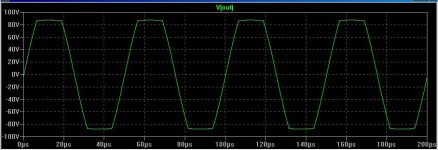
Figure 4 shows the circuits clipping performance at 20kHz. The great clipping performance is courtesty of the simplistic shunt compensation used to stabilise this “single stage” design – there simply are are no complex feedback compensation loops to tame.
Figure 1 is a detailed diagram of the VAS, the VAS buffer and the bootstrapped voltage clamp.
Figure 2 is just a zoomed out screen shot for a topological overview of the (almost) entire amplifier front end. Yes, the circuit is extravagant, but anyone who thinks that it looks complicated just hasn’t seen my +/-90V Vout linear series pass regulator for the (triple EF) power output stage yet.
The diamond buffer is biased by an LM336 2.5V voltage reference. Consequently the (bootstrapped) diamond buffer input transistors run at a healthy Vce of about 3V. To minimised VAS loading, these can be low voltage, high beta types. I’m using BC550C and BC560C in the prototype build.
The bootstrapped isolation diodes (D1 and D3) for the VAS voltage clamp are returned to the opposite terminals of the diamond buffer biasing voltage source. This achieves the operating reverse bias (of ~1.25V) that I mentioned in the last post.
Figure 3 shows just how effective the bootstrapped clamp is. Figure 3 shows the diode currents with the output swinging 160V peak-to-peak, with the diamond buffer driving the 8k feedback resistance.
The red and cyan traces show the current through the bootstrapped isolation diodes, D1 and D3, which are connected to the VAS collector. The green and blue traces, on the other hand, show the current through the actual clamp diodes D2 and D4, which are subject to the full signal swing.
This is the current that would otherwise be loading the VAS, if not for the bootstrapping, or “flying clamp” operation.
At the end of the day I know that this is “just a simulation”, but it is all relative. Here is the linearity performance with the output swinging 160V peak-to-peak, with the diamond buffer actually driving the 8k feedback resistor (which I might add is a much heavier load that the triple EF output stage the real version will get coupled to).
1kHz
Total Harmonic Distortion: 0.000058%
20kHz
Total Harmonic Distortion: 0.000298%
This is achieved with a conservative unity loop gain frequency of 650kHz.
The slew rate is about 160V/us
Figure 4 shows the circuits clipping performance at 20kHz. The great clipping performance is courtesty of the simplistic shunt compensation used to stabilise this “single stage” design – there simply are are no complex feedback compensation loops to tame.
Attachments
Last edited:
Glen,
would you formulate a pleasing phrase for a comment you want to hear, please. Maybe I will use it next time, but no promise. Maybe I`ll just remain silent to hide my ignorance, not to degrade standards with impunity and not to hurt your false pride. Otherwise, you always have the option of not going public or keeping an open mind for your own benefit.
would you formulate a pleasing phrase for a comment you want to hear, please. Maybe I will use it next time, but no promise. Maybe I`ll just remain silent to hide my ignorance, not to degrade standards with impunity and not to hurt your false pride. Otherwise, you always have the option of not going public or keeping an open mind for your own benefit.
Bonsai,
Or both.Either you did grow up next to the lead smelter or you really are just a gadfly.
 Lumba, stop trolling. If you want to contribute technical arguments or data, fine, but anything other than that, you'll be Binned.
Do you intend to build that circuit
Yes. It looks like I'm finally going to have a weekend without being sent away geofizzing by my employer to the middle of nowhere, so I'll have the final board design finished for etching very soon. Anyway, the overtime should pay for all those THAT and SSM arrays I'm going to need..........
Last weekend, 50degC in the shade, solo navigation on the leased land of a uranium mine.... There is no welcoming beach on the other side of that rise.....

Attachments

Last edited:
On the extravagant biasing current sources / mirrors. These are based on THAT arrays, SSM duals and discrete hybrids. This may look over the top, but with 0.01% tollerance emitter degeneration resistors, it's an easy way of generating temperature stable, highly accurate complementary biasing currents, to a fraction of a percent, without any need for trimming.
One thing that I should have also mentioned in my opening post on the folded-cascode "VAS" linearity, is that, for minimum distortion, the "VAS" current needs to be defined by a constant current source, not a biasing resistor.
Otherwise the Vbe variation with signal current of the folded cascode transistor becomes a de-linearising factor.
solo navigation on the leased land of a uranium mine....
You must be glowing in the dark by now.
Nice design, BTW.
Last edited:
Hi Glen
Have you considered adding resistors in parallel with C1 and C2; perhaps 470K or 330K? This would reduce open-loop gain (increasing distortion), but would extend the open-loop bandwidth to 20 or 30 kHz.
Assuming that distortion is more objectionable at high frequencies than at lower frequencies, it seems to me to be of questionable value to pursue lower distortion at low frequencies than at high frequencies.
On the other hand, there may be a benefit in terms of sonic "naturalness" if the characteristics of the amplifier are consistent throughout the audio band.
With distortion around the ppm mark, I doubt it would be audible either way, so perhaps it's more of a philosophical question ...
Any thoughts on the above?
Regards - Godfrey
Hi,
so...there are some authors calling for buffers before and after the VAS. The Hawksford paper (J10) refers to base currents and the alpha factor as the cause of base-collector distortion, advocating a before-buffer cure, apparently originated from the misconception that the BJT is a current controlled device.
Actually, the main cause of the Vbc nonlinearity is the reverse transfer capacitance, which should be principally attended to.
I recently came across this article: Distortion in power amplifiers, Part III: the voltage-amplifier stage | Audio DesignLine
Now I know where the often cited bewildering statements come from.
For me, reading Self is not love at first sight, I have major trouble reconciling myself to his views. Also, building audio amplifier theory upon LTSpice distortion analysis is just not a serious approach. All kinds of distortion should be taken into account, THD is not a universal measure of goodness.
For instance:
And so on...
so...there are some authors calling for buffers before and after the VAS. The Hawksford paper (J10) refers to base currents and the alpha factor as the cause of base-collector distortion, advocating a before-buffer cure, apparently originated from the misconception that the BJT is a current controlled device.
Actually, the main cause of the Vbc nonlinearity is the reverse transfer capacitance, which should be principally attended to.
I recently came across this article: Distortion in power amplifiers, Part III: the voltage-amplifier stage | Audio DesignLine
Now I know where the often cited bewildering statements come from.
For me, reading Self is not love at first sight, I have major trouble reconciling myself to his views. Also, building audio amplifier theory upon LTSpice distortion analysis is just not a serious approach. All kinds of distortion should be taken into account, THD is not a universal measure of goodness.
For instance:
The overall voltage gain is clearly independent of beta. Beta is not part of the equation.The overall voltage gain clearly depends linearly on beta
Or is it?!?! Well, it´s clearly part of the Self-made equation.LF gain = gm x beta x Rc
That´s too optimistic, voltage amplifying stages do distort alarmingly, both buffered and unbuffered. Under dynamic conditions the wondrous virtual static figures will become history, a rather high level of distortions are to be expected from the bandwidth-limited, high open-loop gain, optimally biased blameless architecture. (Eagerly worsened by the triple-Darlington parallel device output).A well-designed voltage amplifier stage will contribute relatively little to the overall distortion total of an amplifier, and if even the simplest steps are taken to linearise it further, its contribution sinks out of sight.
A declining or missing gain and bandwidth does not provide linearity, especially not in voltage amplifying stages. (If it was the case, capacitive feedback would very surely be a generally and widely used linearizing method).at HF the voltage amplifier stage is linearised by local negative feedback through Cdom.
It should make sense even to reputable authors that high open-loop gain comes at the cost of high distortion, measurable or not. It is not the dogma of subjectivists but the dogma of physics.Reducing low frequency open loop gain may be of interest to commercial practitioners but it also has its place in the dogma of the subjectivist.
LTSpice won´t deliver engineering justification. Some form of negative feedback is unavoidable, but considering its potential harmful nature, sharping its edge is ill-advised. Besides, it is not the only weapon to reduce the output stage distortion.Consider it this way: firstly there is no engineering justification for it and, secondly, reducing the NFB factor will reveal more of the output stage distortion. NFB is the only weapon available to deal with this second item so blunting its edge seems ill-advised.
It`s very little about beta, more about transistor type, topology and impedances.As for the input stage, the linearity of the voltage amplifier stage is not greatly affected by transistor type, given a reasonably high beta value.
Current drive will hardly constitute a limitation on the fT of optimally biased output devices.Voltage drive also promises the highest fT from the output devices
Depends on the definition of "linear", but certainly, a balanced voltage amplifier stage has some attractions.but a balanced (and, by implication, more linear) voltage amplifier stage has its attractions.
A very well-founded trepidation.It is right and proper to feel trepidation about inserting another stage in an amplifier with global feedback
Its phase shift is worrisome enough.but since this is an emitter follower its phase shift is minimal and it works well in practice.
And so on...
Hi Glen
Have you considered adding resistors in parallel with C1 and C2; perhaps 470K or 330K? This would reduce open-loop gain (increasing distortion), but would extend the open-loop bandwidth to 20 or 30 kHz.
Assuming that distortion is more objectionable at high frequencies than at lower frequencies, it seems to me to be of questionable value to pursue lower distortion at low frequencies than at high frequencies.
On the other hand, there may be a benefit in terms of sonic "naturalness" if the characteristics of the amplifier are consistent throughout the audio band.
With distortion around the ppm mark, I doubt it would be audible either way, so perhaps it's more of a philosophical question ...
Any thoughts on the above?
Regards - Godfrey
Hi
The effect of the THD dropping with frequency is a function of the open loop gain roll-off, and does not represent any trade-off made in terms if high frequency THD. In fact the opposite is true - a resistor loading the VAS to provide a 20kHz open loop bandwidth would dramatically increase the distortion throughout the entire audio band.
The level of distortion here definately isn't at a perceptible level anyway.
Also, a VAS load resistor to kill the loop gain would also dramatically reduce the PSRR at the lower frequencies (ie mains ripple).
Last edited:
- Status
- This old topic is closed. If you want to reopen this topic, contact a moderator using the "Report Post" button.
- Home
- Amplifiers
- Solid State
- My folded-cascode VAS linearity investigation