Bonsai,
They have not.I have no expereince with mosfets in the VAS, but I imagine they have some very useful properties in the type of circuit we are talking about here.
Yep, pretty extensively simmed and built the Haksford cascode, Baxandall
pair and a self improvised X coupled darlington arrangent.
They all do pretty much the same thing - re process the base current and
non linear bc capacitance. They are all susceptable to oscillation, especially
the Baxandall pair, probably because the 'clean up' transistor works with
very little head room. In the event of oscillation, decoupling the 'clean up'
transistors base to ground at VHF usually works but not always.
I like this topology applied to a power amp but unforunately when you
substitute that ideal infinite current gain OP stage on your sims for a real
one, all those really cool distortion numbers get shot to pieces.
Then the design task becomes more - what OP stage can I put with the
Hawksford VAS to preserve it's merits. This becomes a much more tricky
task.
Good thread Glen.
cheers
Terry
I agree about the potential stability issues with the “Hawksford cascode” VAS, but with the addition of a base stopper and/or an emitter resistor for the cascode transistor, I’ve never had an issue with parasitic oscillation (even in crappy dead-bug prototypes with rather poor “layout”).
The folded cascode VAS is sensitive to non-linear loading, but I’ve achieved results about as good as one could want by buffering it with a bootstrapped diamond buffer (where the collectors of the pre-drivers are returned to the emitters of the output devices). This is before a triple EF OPS.
I've played with a CFP VAS buffer (as in the ExtremeA amplifier), but it isn't as good and too finiky WRT to parasitic oscillation to my liking. The bootstrapped diamond buffer seems to be easy to tame with base/collector/emitter "stopper" resistors.
Last edited:
Glen,
the investigation needs to be completely remade from scratch.
Although immense efforts have been devoted to designate the functional determinants in the bipolar junction transistor, false explications are flourishing. The chances to make novel discoveries are thin, even if you know what you are doing. Those THD figures are not meaningful, dynamic behavior is. Compose yourself, take your time, and come back later. Again, I`ve seldom seen so much rubbish compressed in just one post.

Then the design task becomes more - what OP stage can I put with the
Hawksford VAS to preserve it's merits. This becomes a much more tricky
task.
Here is a simplified diagram of how I buffer the VAS and implement a bootstrapped anti-saturation VAS voltage clamp.
D2 and D4 are the clamp diodes proper while D1 and D3 are the isolation diodes. D1 and D3 are bootstrapped by R1 and R2, having their A-K potential maintained at 0V until the clipping point at which either D2 or D4 become forward biased.
This effectively isolates the non-linear junction capacitance and leakage currents of the clamp diodes from the sensitive VAS node.
Attachments
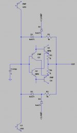
That was just a simplified schematic to demonstrate the bootstraped clamp operation. However there are issues to overcome.
When the diamond buffer is called upon to deliver current, a voltage drop is developed across one of the output emitter resistors (R3 and R4). This means that the output voltage of the diamond buffer will be either slightly higher or slightly lower than the input voltage to the diamond buffer.
If the load current is sufficient, this will cause either of the bootstrapped clamp isolation diodes to become forward biased, thus loading the VAS.
The trick to avoid this issue is to run each bootstrapped isolation diode with a small (a volt or so) reverse bias. Later when I have the time I’ll export my Protel schematic showing the non-simplified VAS buffer and clamp circuit which achieves this (and also increases the operating voltage of the diamond buffer input transistors with a biasing voltage source at the input, between the transistor bases).
Last edited:
Aesthetically displeasing? What are you talking about?
Get used to our Spambot.
- Status
- This old topic is closed. If you want to reopen this topic, contact a moderator using the "Report Post" button.
- Home
- Amplifiers
- Solid State
- My folded-cascode VAS linearity investigation