Oh, I wish I had the time to really work on it but I've currently got the old
Tiger amps in the que to do. Not a priority, just for the enjoyment.
The first and second gain stages in that design look reasonable, I'd add
bootstraping, and the top half of the output stage emitter follower looks
reasonable, a bit strange but more or less reasonable.
The lower half is, what? A sliding current source? I'd have to simulate it
to get more insight.
Pete B.
HI all
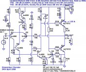
Surely some mistake in the diagram?
The second stage diff pair is a class A to drive the output stage in class A, but it seems to me that the left hand decoupling capacitor (between 2.7k - 390 tap) should be bootstrapped while the right hand should go to ground. Don't think this is a sliding bias- just a push pull class A?
And it would probably be a lot better with newer transistors...
all those roll-off capacitors probably mean it has a high susceptibility to overloading the input stage at high frequencies....
cheers
John
Possible, because the upper output NPN's base is dynamicly changing (follower) while the lower output NPN's base is relatively steady.The second stage diff pair is a class A to drive the output stage in class A, but it seems to me that the left hand decoupling capacitor (between 2.7k - 390 tap) should be bootstrapped while the right hand should go to ground.
Hi Lumanauw
...in which case the 4.7 ohm filter resistor and second 2200 uF capacitor in the psu are not needed.
Here's what I suggest: the original circuit probably is intended to run with "fixed" collector loads, because the left hand side needs a higher voltage to make sure there is enough drive for the upper output stage.
The bootstrapped right hand side makes sure that the RHS sees the same load as the LHS. But this arrangement forces the diff pair to swing through almost all of its operating conditions. I estimate that the diff amp transistors run at 7 mA and have to swing between 1 and 13 mA to get full output.
Changing the bootstrap sides over has some advantages: the additional voltage on the LHS is not needed, so the PSU filter is not needed, and higher output power can be achieved with the same psu. In addition the current swing in the diff pair is reduced to be only approximately that of the base current needed by the drivers, i.e. about 1..2 mA, improving linearity and lowering distortion.
Only trouble is that, as with JLH69, any increase in base drive on one side is achieved by a reduction in base drive from the other, so if you use transistors with a gain which falls with increasing current (2N3055 for example) the quiescent current has to be set a little higher than half the peak output current
Cheers
John
Hi, John,
Thanks for the advice. I also think changing the topology like you suggest is better, changing bootstrapp from left to right.
I'm thinking about using slow transistors throughout the amp for small transistors (MJE340-350 for all small transistors, 3-4mhz) and 30mhz for output (2SC2922). Will this give problem?
john_ellis said:HI all
Surely some mistake in the diagram?
The second stage diff pair is a class A to drive the output stage in class A, but it seems to me that the left hand decoupling capacitor (between 2.7k - 390 tap) should be bootstrapped while the right hand should go to ground. Don't think this is a sliding bias- just a push pull class A?
cheers
John
I am not sure if it was intended to have it as a sliding class A . I personally would basically design it as you have proposed, but the mullard design seems to do it different on purpose. Have a look to the voltage rating of that 220uF bootstrap cap, 6.3V. This is fitting to the bias settings of all stages. If intended to be put to GND the voltage rating should be min 30V, better 50V. For me it is looking like Mullard intended to run the lower half mostly as a constant current source... but then I am wondering how we should get output currents above 1A without clipping... What's the opinion of PSPICE? As In understood there are already some simulations around...
Hi chocoHolic
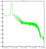
Yes I agree that the circuit probably was deliberately designed the way it was published, but I simulated the distortion as was and with the bootstraps swapped. CUriously, the distortion as was at about 15V output was 0.35% but with the swap, was <0.1% at higher output. If you swap the bootstrap side, then it will be necessary to choose the right voltage of capacitors.
Hi Lumanauw
I would not recommend MJE340's in the input stages - my usual input stage transistors are BC307 (PNP) or BC237 (NPN). Once these were made with the TO-18 triangle pin-out but as manufacturers have sought to lower costs the pin-out is now in line like many TO-92's. BC547, BC557 are similar. For the diff-pair VAS with the swapped bootstrap you could use BC546 rated at 60V or BD139's, as you could reduce the current a little to say 5..6 mA in each side.
Calculations of the optimum resistors needs some thought. I'll publish my conclusions later.
Cheers
John

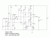
 a little bit more about this circuit...
Hi Lumanauw, chocoholic
Here's my proposal for a mod version of this amplifier.
Some comments: I have used BD139s for the drivers and diff-vas.
I prefer these to MJE340's because they have higher fT and gain. The MJE340's seem to me to be like old video transistors - fine at high voltage, but for linear apps tend to have ft limitations below 10V because of the epi. BD139's also have a low voltage ft-reduction but this tends to be below 5V rather than 10V.
The driver stages keeps the capacitor bootstraps but the load resistors are split. To improve LF response, the capacitors all need to be bigger than in the original. But with capacitors directly connected to the collectors of the drivers, a short circuit could cause discharge - especially if bigger values are used- which might kill the o/p transistors. With the split load resistor, short circuit output current is limited, admittedly dependent on the gain of the output transistors, to about 5 or 6A.
The output capacitor is increased to 4.7 mF - this is better for LF, but the decoupling bias capacitor needs to be 22 mF to keep pace. But with modern low-R, low-Z capacitors a few parallelled 4.7 mF might be fine.
Frequency compensation uses the phase-lead approach John Linsley Hood and Bailey adopted (and the method I prefer). The input filter is split into separate frequency-stability concerns and actual HF filter. THe first RC pair (2.2k, 330 pF) are to prevent input stage overloading at high frequencies, the second is to provide stability (the 330 pF is too high). By all means if you think the input filter ruins audio performance you can take this off, and most audio material won't cause TIM in any case.
I noticed during simulations that there is a sliding bias effect. Unfortunately this is in entirely the wrong direction. The quiescent current DROPS in both output transistors, at the start of a signal, and this means that to stay in class A the quiescent current has to be quite big. Hence the reason for the 1.5 ohm and approx. 2A quiescent current. But this amp gives 25W into 8 ohms at 0.02% distortion which is only 2nd harmonic, no evidence of crossover distortion (as there should not be).
Think this is better than the original but I hvaen't tried it for real yet.
cheers
John
Attachments

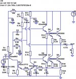
Some further modifications to the version by John Ellis above - the main changes are the removal of the bootstrapped collector loads of the drivers, yielding a true darlington O/P stage; doubling the 2N3055 outputs to keep it well within SOA limits; and minor biasing changes that yield better THD20 numbers. At +/- 20V output swings (25W into 8 ohms), it simulates with H2 ~= -72 dB and H3 ~= -90 dB, with much better numbers for smaller swings; H2 dominates H3 throughout by 18 dB or better - in short, a worthy contender to JLH Class-A derivatives.
Further mods could involve heftier outputs like 2N3773 or 2sc5200, with higher rails; or lower-end integrated darlingtons like TIP142 or similar and lower rails.
Further mods could involve heftier outputs like 2N3773 or 2sc5200, with higher rails; or lower-end integrated darlingtons like TIP142 or similar and lower rails.
Attachments
Here's the LTSpice schematic of a darlington output version with lower rails. It can deliver about 15W into 8 ohms, with simulated THD20 numbers showing H2 at ~-85 dB, H3 at ~-95 dB and everything else below -100 dB. There's nothing special about the output device - it could be substituted with a TIP142, BDX33c, 2N6059 or similar, as long as the SOA is not exceeded.
Edit: The bc850 and 858 devices are SMT versions having the same die as the bc550 and 558 - there's no difference in their behaviour/Spice models.
Edit: The bc850 and 858 devices are SMT versions having the same die as the bc550 and 558 - there's no difference in their behaviour/Spice models.
Attachments
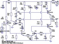
Some further changes to the darlington version above - a few changes to the LTP stage in the form of a few small-signal transistors improve the distortion numbers dramatically!
It now simulates with H2 at ~ -106 dB at 14W into 8 ohms, Class A. It can also drive a 4 ohm load, but only in Class AB, with H3 dominating at -96 dB. This is now arguably the lowest distortion amplifier on this forum with a BOM of ~$5/channel - it should beat most of the JLH-derivatives hands down.
For more H2 (higher distortion, but pleasant), just replace the CCS consisting of R11, Q6, Q7 and R21 with a single 5.6K resistor - this restores the tanh() character of the input LTP.
Here's the latest version:
Attachments
Siva,
Thank you for your wonderful work on this seminal circuit. I've always liked it, and you've shown us all how good it really is.
Do you think this circuit could be expanded to higher power easily? It's one thing to create a low power amp of exceptional performance, but the real test comes at greater than 100W. I seem to remember it ran around 1.1A quiescent at 45V on the original circuit in Elektor; at 100V, for a true 100W into 8R, you'd need to more than double this current and dissipation would doubtless require some very heavy duty heatsinking.
Cheers,
Hugh
The main limiting factor is the SOA of the output devices - I went with inexpensive 'industrial grade' darlingtons to keep the costs down. However, these could easily be substituted with discrete darlingtons consisting of (say) Sanken output devices with much higher SOA, paralleled if necessary, with higher rails and higher quiescent current. I see no difficulty in scaling it to 100W, with suitably dimensioned heatsinks - but it would also double as a moderately large room heater. Probably OK for the temperate regions of the planet, harder to justify in the tropics.
Hi Siva
I agreewith your updates.I onlykept�@the bootstrap�@on the drivers to keep the low power devices of the original.
I recommend using discrete driver and outputs in the updated circuit. Most Darlingtons have poor SB compared with separate outputtransistors.
cheers
John
I agreewith your updates.I onlykept�@the bootstrap�@on the drivers to keep the low power devices of the original.
I recommend using discrete driver and outputs in the updated circuit. Most Darlingtons have poor SB compared with separate outputtransistors.
cheers
John
Hello, I have been looking at this thread with interest, in particular the first, "how does this amp sound". It's evolved quite a bit since then. It's not unlike a circuit I designed and am using, and if anyone is interested I could post the schematic. And as to how does it sound, ABSOLUTELY WONDERFUL, it has that magical quality that draws you into the performance, it is truly "compelling listening" as I call it. And if anyone would care to simulate it I would be fascinated to know how it performs in a simulation. I know what my ears tell me.
Regards Karl
Regards Karl
- Status
- This old topic is closed. If you want to reopen this topic, contact a moderator using the "Report Post" button.
- Home
- Amplifiers
- Solid State
- Mullard SS power amplifier