For example:
page 8 of this datasheet, under simplified schematic.
http://www.lcaudio.dk/comp/ad846.pdf
page 8 of this datasheet, under simplified schematic.
http://www.lcaudio.dk/comp/ad846.pdf
Scopes
I might just add that I bought a TDS210 digitising scope after my analog Hitachi broke down. The TDS is difficult to work with though it can do a few nifty things. I had to go out and buy an analog scope within a month ! Suggest you stick to analog scopes unless you want storage and other facilities .
I might just add that I bought a TDS210 digitising scope after my analog Hitachi broke down. The TDS is difficult to work with though it can do a few nifty things. I had to go out and buy an analog scope within a month ! Suggest you stick to analog scopes unless you want storage and other facilities .
Re: Scopes
Thanks for your info. I determined to buy Protek analog 20MHz scope.
JH
ashok said:
Suggest you stick to analog scopes ...
Thanks for your info. I determined to buy Protek analog 20MHz scope.
JH
Re: Scopes
scope is still good to have around.
I keep a TDS210 around. It's a good enough scope for everything except seeing the vaguest oscillations, and it particularly excels at capturing and hold high musical voltage/current peaks, making it particularly good for looking at amplifiers into speakers with music. But you're right, a fast analogashok said:I might just add that I bought a TDS210 digitising scope after my analog Hitachi broke down. Suggest you stick to analog scopes unless you want storage and other facilities.
scope is still good to have around.
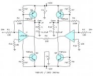
Probably could be made to work. Assume you will end up trimming the values and dealing with compensation. I would put about 10K to ground on each - input, right off the bat, and probably an RC to ground at each output.jh6you said:Your "Yes" or "No" would much appreciate.
Component values
Hi JH,
How did you arrive at the component values in your circuit? I figured values that were quite different. I will explain how I got mine .
The resistors in the base emitter of the transistors, R5.R6.R7.R8.
The dc bias current of the opamp will generate a voltage across these. The LM353 has a supply current rated 3.6 to 6.5mA. Taking a 5mA value and 1.1 volt Vbe for the Darlington TIP's , this turns out to be 220 ohms. You cannot turn on the transistor in the no signal condition as there is no current control on it.
To fully turn on the transistors you will need about 1.5 volts Vbe.
This will mean that we have a current of about 6.8 mA flowing through the R5,6,7,8. The signal component of this would be about 6.8-5 mA ~ 1.8 mA. This is well within the capability of the opamp.
It is not clear about the opamp output voltage when the transistors are fully turned on. With 100 ohms that would be about 90mV at the output of each opamp. Wouldn't that be comparable to dc voltage errors at the output of the opamp which may be several mV in open loop. I am not thinking clearly I guess.
As a guesstimate I would use say at least 2 volts output on the opamp to drive the TIP's fully on. So I would probably try about 2 or 2.2K ohms for R0.
You will also have to use the resistors from the + input to ground, as mentioned in Nelson's post , as it will reduce dc offsets.
How about your approach?
Cheers.
Software for TDS210
Hi Nelson,
Sorry for hijacking this thread for something off track.
Did you ever consider buying ( or already have ) the software bundle that comes with the TDS210 RS232 port adapter or the Wavestar software. Are they any good , meaning are they really flexible , FFT etc?
Thanks.
Hi Nelson,
Sorry for hijacking this thread for something off track.
Did you ever consider buying ( or already have ) the software bundle that comes with the TDS210 RS232 port adapter or the Wavestar software. Are they any good , meaning are they really flexible , FFT etc?
Thanks.
back to work: tda7293
This gainclone thing has a pin between driver and power stage (pin11) and separated power supplies for both stages, perhaps usefull in these configurations, at least better tracking when using the power supply-modulation of power stage.
Maybe with some voltage supply level tricks we could go further.
There's no schematic of the whole internal kitchen so just guessing...
my 2 cents.
http://schematic.info/Docs/tda7293.pdf
Re: Component values
I am a kind of hopeless man about the electronic circuit analysis. So, I have to spend much time after work to understand the basic of electronics. This is also a good excuse to avoid TV news about the bloody hell of politicians.
You are right. We could turn on the TIP with Vbe of about 1.4V (not 0.7V as I initially thought). Therefore, we will get the supply voltage of 8.6V to LF353, and the corresponding typical supply current of about 3.4mA according to the data sheet. I assume this 3.4mA as a current source. Meanwhile, I want to have a base current of about 1.6mA to the TIP. Then, the remaining 1.8mA is to be used to generate 1.5V across the base and the emitter. This requires R5 of about 787. I consider R5 as a sort of bootstrapping resistor. Please note that all these are based on the first approximation. So, the correct values might be somewhat different. What would happen if the supply current is going crazy up to 6.5mA? I would go crazy, too.
I might be wrong. I am however relaxed to some degree because Nelson Pass will as usual thunder in and light the garbage off.
R0...? Pwhoooo... I do not know... I just understand the value as Nelson Pass says--to be compromised in consideration of the stability and the distortion.
JH
ashok said:
How did you arrive at the component values in your circuit?
I am a kind of hopeless man about the electronic circuit analysis. So, I have to spend much time after work to understand the basic of electronics. This is also a good excuse to avoid TV news about the bloody hell of politicians.
You are right. We could turn on the TIP with Vbe of about 1.4V (not 0.7V as I initially thought). Therefore, we will get the supply voltage of 8.6V to LF353, and the corresponding typical supply current of about 3.4mA according to the data sheet. I assume this 3.4mA as a current source. Meanwhile, I want to have a base current of about 1.6mA to the TIP. Then, the remaining 1.8mA is to be used to generate 1.5V across the base and the emitter. This requires R5 of about 787. I consider R5 as a sort of bootstrapping resistor. Please note that all these are based on the first approximation. So, the correct values might be somewhat different. What would happen if the supply current is going crazy up to 6.5mA? I would go crazy, too.
I might be wrong. I am however relaxed to some degree because Nelson Pass will as usual thunder in and light the garbage off.
R0...? Pwhoooo... I do not know... I just understand the value as Nelson Pass says--to be compromised in consideration of the stability and the distortion.
JH
Attachments
jam said:A pair of these, correctly biased should work nicely in this application. The Hiraga 20w class A also comes to mind.
Jam
I was skimming through the thread from start yesterday and
had another look at this Current-feedback power amp you
posted awhile back and found it interesting. Do you have any
more info about it, or a link or whatever?
For me the basic X circuit with CF opamps on page 1 popped one idea in my mind.... Is't this a perfect circuit to use with balanced output bitstream DAC chips. With this schematic it seems to be possible to make a filter for which both outputs of the DAC see absolutely the same load and if filter components are very closely mached it could provide superb results.
But here question to Nelson (or anyone else who knows the answer) - will this circuit be stable if one builds a 3rd order active filter around it
Ergo
But here question to Nelson (or anyone else who knows the answer) - will this circuit be stable if one builds a 3rd order active filter around it
Ergo
JH,
I explained how R0 could be worked out. The load current through R0 will come through the resistorsR5,6,7,8 depending on which device is 'on'. So it will increase the drop across these resistors providing the voltage the base emitter requires.
The maximum base current should be about 0.5mA at maximum collector current of the power devices. Hfe at about 1.5 amps is quoted at "typically" x3000. Someone should build one and try it out. Anyone ?
Ergo ,
The circuit has a differential input and differential output with a floating load. How would we make a 3rd order filter with this configuration. Is the intended application to be a line level filter or a 3rd order filter built around the power amp. Interesting idea.
Cheers.
Having virtual ground inputs, X circuits are fairly ideal for balanced DACs based on current sourced outputs. Just eliminate the input series resistor. You can get your first pole using a capacitor in parallel with the feedback resistors, and the remaining poles are best done passively.
Christer,
Check out
http://perso.wanadoo.fr/jm.plantefeve/
beware it is in French. I will try to locate and post a few more current feedback circuits.
Jam
Check out
http://perso.wanadoo.fr/jm.plantefeve/
beware it is in French. I will try to locate and post a few more current feedback circuits.
Jam
jam said:Christer,
Check out
http://perso.wanadoo.fr/jm.plantefeve/
beware it is in French. I will try to locate and post a few more current feedback circuits.
Jam
Great, thanks. That guy seems to love current-feedback amps
with lateral MOS-FET OPS's. Most of the amps were a variation
on that theme.
Test Version
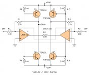
No. I can't use the dual op amp LF353 as it has a common voltage supply for the two channels. Therefore, I select two LM741 op amps (typical supply current of 1.7mA). And, for the power booster transistors I choose TIP141/146 (on-Vbe about 1.4V). The values of R5/R6/R7/R8 are decided with 1k. If this test circuit works as I wish, I would get output power of 22W per channel.
By the way, for the test of this circuit, is the regulated rail voltages recommended?
JH
PS
If this test version has no hope, please tell me so. I would much appreciate it.
Attachments
- Status
- This old topic is closed. If you want to reopen this topic, contact a moderator using the "Report Post" button.
- Home
- Amplifiers
- Pass Labs
- Monolithic SuperSymmetry with Current Feedback