I see now, it lets the brakes off the gain at DC so it corrects the DC offset to a fine degree, so either a manual pot somewhere would have to trim it, or a DC servo added.
Even a trim pot wouldn't be a perfect solution because the amp (in common with most discrete designs) has no pretensions of DC precision. Yes, you could trim the offset but it would wander all over the place with any temperature and rail voltage variations.
A servo would probably work well but tbh the cap in the feedback return is the best answer to the problem. Beatties... wasn't that a model shop. I remember the name.
Agreed - the 47uF cap is a neat solution. I've added a 1uF bypass cap to the (polarised) electro cap now, I didn't have a non-polarised cap - I thought about two 100uF back to back, but not implemented that.
Yes, Beatties was the model shop, RC Tamiya and Acoms goodness! The 1980s allowed one to be very creative..
This is a 'using bits I have' tidy up project - rather than a 'buy new bits' project, so what's around tends to get used
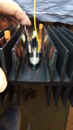
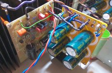
Squashed some 1000uF 63V caps on as they were the only 63V ones I had, on their sides, to reduce height of the board. The sideways cap is because that centre hole is needed to hold the board to the new heatsink. Glued with silicone blob.
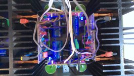
Boards are slightly different, one (LHS) had conformal coating - but it seems to be genuine as I can solder through it Ok.
I also bypassed the bias pot with a 560R resistor as in testing they needed about 200R for a 100mA bias.
Gate stopper resistors are 270 Ohms, can't recall any other mods needed ?!
Found an old pair of WIMA 1.0uF caps for input for neatness. 5W 4R7 resistors replaced as the old ones were a bit baked. Most builders fitted them too low, including me, so they scorch the PCB. Boards will be vertical, terminals at the top, so any heat won't cook the capacitor.
..Probably the snubber shouldn't get too warm if nothing nasty is fed to it. I did discover my old Moto E6 mobile seemed to have a lot of energy at the headphone socket at about 450kHz so I stopped using that as a signal generator now
Next task to clean up and mount the old transistors!

Yes, Beatties was the model shop, RC Tamiya and Acoms goodness! The 1980s allowed one to be very creative..
This is a 'using bits I have' tidy up project - rather than a 'buy new bits' project, so what's around tends to get used
Squashed some 1000uF 63V caps on as they were the only 63V ones I had, on their sides, to reduce height of the board. The sideways cap is because that centre hole is needed to hold the board to the new heatsink. Glued with silicone blob.
Boards are slightly different, one (LHS) had conformal coating - but it seems to be genuine as I can solder through it Ok.
I also bypassed the bias pot with a 560R resistor as in testing they needed about 200R for a 100mA bias.
Gate stopper resistors are 270 Ohms, can't recall any other mods needed ?!
Found an old pair of WIMA 1.0uF caps for input for neatness. 5W 4R7 resistors replaced as the old ones were a bit baked. Most builders fitted them too low, including me, so they scorch the PCB. Boards will be vertical, terminals at the top, so any heat won't cook the capacitor.
..Probably the snubber shouldn't get too warm if nothing nasty is fed to it. I did discover my old Moto E6 mobile seemed to have a lot of energy at the headphone socket at about 450kHz so I stopped using that as a signal generator now
Next task to clean up and mount the old transistors!
I remember my first Maplin lateral mosfet amp around 1980.
It went together well.
The pre drilled transistor mounting bracket was very helpful.
The previous build of a 225WRMS Maplin disco amp the heat sink didnt come pre-drilled and was very hard to drill accurately.
It went together well.
The pre drilled transistor mounting bracket was very helpful.
The previous build of a 225WRMS Maplin disco amp the heat sink didnt come pre-drilled and was very hard to drill accurately.
hello NigelThe 47uf gives an AC short while not shorting DC.
This gives an AC gain but not a DC gain which gives more stability.
Just sent you a PM
Hi Folks, I've got another question about the schematic, well, about a variation of it..
I'm feeding + and - to the mosfets via a 'separate bridge+caps module', than the driver part. So the + and - goes to the MOSFET drain pins, and the sources (cases) go to the speaker, then the speaker return goes to the earth on the 'separate bridge+caps module'. Completing the current loop: PSU + speaker + MOSFETs.
This then isolates the speaker currents from the rest of the amplifier circuit, apart from the feedback from the sources to the LTP via the 33k resistor.
But... the snubber, R15 + C7, I guess (?) is there to soak up any dodgy HF/RF getting through that far, goes from the sources to ground. But this ground is my signal ground, not the speaker(power) ground from the 'separate bridge+caps module'.
So I don't really want this stuff waggling my signal ground, but to move it to the power ground, requires (yet) another wire - so I was wondering if I can connect that end of R15 to a power rail instead?
Ie: it's an AC path (due to C7), so does it really matter if it goes to a power ground or a power + or - terminal?
Thanks in advance
Hi all, just an update for my Maplin MOSFET in an F6B project!
I may do a different thread on the F6B conversion as it has it's own questions and challenges, so just the MOSFET stuff here.
But I will mention that due to the original having mains earth to chassis and the power supply earths also as the chassis, and me having mains earth to the chassis, and all signal earth isolated (via a 120R with X2 in parallel) the Sony habit of running the ground around (one ends of many shields being left open) did required some taming, some of which I don't fully understand.
The GNFB of the mosfet amp prevented my 'Plan A' of isolating power earth and signal earth completely, so (Plan B) they come together in the middle of the 'box', which is then used for the pre-amp ground references for left and right, while the old pre-amp power ground is tagged off to the PSU filter that supplies it. Trying to get currents all into twisted pairs.
One day if I can get an LTSpice model working I'll investigate a no GNFB version so I can use a decent grounding system .
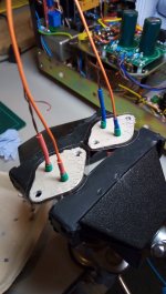
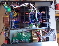
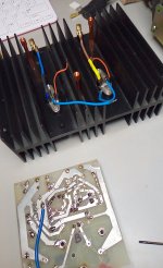
The 6.3mm spades are for the MOSFET drains, the gates are stuck through (holes drilled in) the board and soldered to the 300R gate resistors (see last pic), the sources are then soldered to the PCB as usual, via wires.
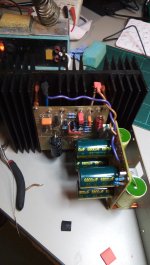
Grounding again dictated I use the local PSU filters for the driver section too, so a Schottky and 39R feeds each rail into 1000uF caps on PCB, to isolate it from the music dips.
The PSUs filters are GBJ2510 bridge in 4 x 6,800 uF caps with 22uF films to bypass, as I had them. Bias is about 100mA, the heatsinks are much nicer than usual, so I think dynamics are better as the lateral MOSFET doesn't heat up so fast with this heatsink.
The main PSU is a toroid, probably about 200VA, perhaps a little more, soft start with 56R for 240V, speaker protection module, on really loud stuff the rails sag just over 1V so it seems Ok, lots of 'strength' behind the sound.
Not had much runtime but it does sound nice, very listenable, and finally those old rusty MOSFETs are again in use, weaving their magic
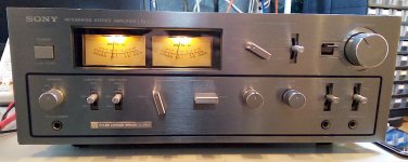
I can recommend the Sony as a box for this type of project, some people preserve the old pulse PSU: for replacement I was going to use two switchers, but could not guarantee a decent quiet switcher and I had a spare toroid. The heatsinks are nice and while the Sony is 'wildly over-engineered' with all those crazy (top top quality) wires going back to front, I prefer the Maplin MOSFET design over the slightly boring BJT in the sony, even though the old power amplifier in there actually worked... But for how long?... it used sockets for the TO3 devices - horror, so I modified them for soldered wires (see pic 1) and the MOSFETs are soldered.
The GNFB capacitor - the 47uF one I eventually bypassed with an 820n and switched for two 100uF caps in series - doubling the breakdown voltage.
Max voltage across it will be I think 50V / (33k/1k) = 1.5V and they don't conduct as diodes until 1.0-1.5V each.
I also added a 120R resistor into a 220pF capacitor on the inputs. The 120R stops an inexplicable hum issue at zero volume (that seems to invite the amplifier to amplify the difference between two slightly different grounds, but no idea why a small resistance stops it..), and the cap reduces a bit of RF that I seem to have around my workbench, not sure where it's from as with everything switched off it's still there.
I may do a different thread on the F6B conversion as it has it's own questions and challenges, so just the MOSFET stuff here.
But I will mention that due to the original having mains earth to chassis and the power supply earths also as the chassis, and me having mains earth to the chassis, and all signal earth isolated (via a 120R with X2 in parallel) the Sony habit of running the ground around (one ends of many shields being left open) did required some taming, some of which I don't fully understand.
The GNFB of the mosfet amp prevented my 'Plan A' of isolating power earth and signal earth completely, so (Plan B) they come together in the middle of the 'box', which is then used for the pre-amp ground references for left and right, while the old pre-amp power ground is tagged off to the PSU filter that supplies it. Trying to get currents all into twisted pairs.
One day if I can get an LTSpice model working I'll investigate a no GNFB version so I can use a decent grounding system
.The 6.3mm spades are for the MOSFET drains, the gates are stuck through (holes drilled in) the board and soldered to the 300R gate resistors (see last pic), the sources are then soldered to the PCB as usual, via wires.
Grounding again dictated I use the local PSU filters for the driver section too, so a Schottky and 39R feeds each rail into 1000uF caps on PCB, to isolate it from the music dips.
The PSUs filters are GBJ2510 bridge in 4 x 6,800 uF caps with 22uF films to bypass, as I had them. Bias is about 100mA, the heatsinks are much nicer than usual, so I think dynamics are better as the lateral MOSFET doesn't heat up so fast with this heatsink.
The main PSU is a toroid, probably about 200VA, perhaps a little more, soft start with 56R for 240V, speaker protection module, on really loud stuff the rails sag just over 1V so it seems Ok, lots of 'strength' behind the sound.
Not had much runtime but it does sound nice, very listenable, and finally those old rusty MOSFETs are again in use, weaving their magic
I can recommend the Sony as a box for this type of project, some people preserve the old pulse PSU: for replacement I was going to use two switchers, but could not guarantee a decent quiet switcher and I had a spare toroid. The heatsinks are nice and while the Sony is 'wildly over-engineered' with all those crazy (top top quality) wires going back to front, I prefer the Maplin MOSFET design over the slightly boring BJT in the sony, even though the old power amplifier in there actually worked... But for how long?... it used sockets for the TO3 devices - horror, so I modified them for soldered wires (see pic 1) and the MOSFETs are soldered.
The GNFB capacitor - the 47uF one I eventually bypassed with an 820n and switched for two 100uF caps in series - doubling the breakdown voltage.
Max voltage across it will be I think 50V / (33k/1k) = 1.5V and they don't conduct as diodes until 1.0-1.5V each.
I also added a 120R resistor into a 220pF capacitor on the inputs. The 120R stops an inexplicable hum issue at zero volume (that seems to invite the amplifier to amplify the difference between two slightly different grounds, but no idea why a small resistance stops it..), and the cap reduces a bit of RF that I seem to have around my workbench, not sure where it's from as with everything switched off it's still there.
Attachments
-
 IMG_20240107_210440_569.jpg387.4 KB · Views: 65
 -
 IMG_20240107_185111_701.jpg329.2 KB · Views: 70
 -
 IMG_20240123_175855_671.jpg370.8 KB · Views: 68
 -
 IMG_20240207_132024_602.jpg512.1 KB · Views: 64
 -
 IMG_20240207_131954_341.jpg416.6 KB · Views: 68
 -
 IMG_20240207_131943_368.jpg303.5 KB · Views: 70
 -
 IMG_20240130_192155_248 copy.jpg403.7 KB · Views: 71
excellent work, never has the Sony sounded so good One thing that is quite important (and I can't quite make out if you have done this with all that sleaving) is to place the gate stopper resistors as close the FET's as possible. It can be very important to keeping things stable.
They were a curiosity back in the day but are grim in many respects. The toroidal is to be much preferred.some people preserve the old pulse PSU
Thanks, interesting, I knew this for tubes for forgot for MOSFETSas close the FET's as possible
They are probably 30-40mm away now, short of listening and seeing how hot the snubber resistor gets - what's a good way to check stability? See if a square wave rings into a speaker load?
If I take them to bits ever I can put them closer, hoping to avoid that unless I measure any ringing
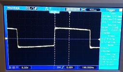
Squarewave
Hi all, I checked it with a nice 200Hz square wave and all is good, except for the usual RF noise that appears even when everything is switched off.
I must track that down!!
Testing revealed what goes in, comes out, even a square wave driving a distant speaker.
I actually cut the traces on the PCB so perhaps the overall length of gate wires is not much different from the longest PCB gate trace, and it's fair straight, direct wire.
I had a read of the TI PDf called 'Fundamentals of MOSFET and IGBT Gate Driver Circuits'
The most difficult task in direct gate drives is to optimize the circuit layout. As indicated in Figure 8, there might be considerable distance between the PWM controller and the MOSFET. This distance introduces a parasitic inductance due to the loop formed by the gate drive and ground return traces, which can slow down the switching speed and can cause ringing in the gate drive waveform.
So perhaps the local driver board PSU bypass capacitors could be better placed, near the gate drives..
I did discover the 'reverse/stereo/L/R/mono control was a bit noisy, but that's an F6B thing
That all sounds promising tbh and it sounds like you haven't any obvious issue. Inductance of the wiring (and it interacting with the junction capacitance of the FET) is the problem.
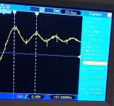
Just doodling with the sim. Gate stoppers removed and small inductance added. This is the kind of thing that can happen.

Just doodling with the sim. Gate stoppers removed and small inductance added. This is the kind of thing that can happen.
Very interesting! I can see it forms a tank-circuit and rings like a bell.This is the kind of thing
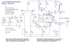
Would it be possible to post the LTspice ASC file and models for this amplifier please? I want to try a few things with it, but without having to take it all to bits etc
Thanks, this is awesome. On the Mac the asc files now even show up as icons, so a simple double click and it's there, open and runnable.run as is
Thanks again
I had a problem with one of the bias adjusters, the top rotating bit seemed to lose interest in being electrically connected to the track, so I've ordered a couple of nice 470R adjusters to replace them (Which will be bridged a little with a 560R and 1.8K as I need 168R and 208R), but this meant I had to pull the boards (doh!), and while out I can change the 22pF for 33pF, and the 47pF for a 330pF (simulated OK - thanks again), re-fit the big snubber resistor..
... and contemplate moving the gate stoppers closer. So I was really asking about the physics of the stopper - closer to the gate = less capacitance .. on that (high impedance) side of the stopper?
As is the copper wire (orange) has no real capacitance to add to the gate capacitance, and I guess on the 'left' is where inductance is an issue (between the driver and the stopper), which will be largely unchanged.. I'm not sure it's worth moving the stoppers.
The scope traces are from the other day, driving a square wave in from an iPod Touch (which has a 20kHz 'ring' in it anyway, so ignore that bit), to a speaker. It's 'clean', apart from the speckle of RF I get in that location, as you can see, which seems like the combination of my scope and metal items, it's even there when the amp is powered down - hence my keen interest in RF suppression.
On the scope, that RF looks like packet based speech... but at 15MHz or so. Very odd.
In other news, the strange ground noise I had a zero volume (when the input pin was grounded by the 10K volume pot), was solved (but not explained) by a relocation of the F6B pre-amp PSU ground wire to that PSU filter, and the addition of a 120R input resistor. As I changed two things at once (yes, I know LOL), I was not sure what the cure was, but looking at the Maplin circuit more closely, the 1uF cap C1 runs into a 2.2k resistor anyway - so clearly my 120R resistor is bogus. So that cure was the removal of a small, but audible current path.
Then I looked at the F6B schematic again, and their power amp has no input capacitor - no need - so I'm also eliminating C1, and replacing R1 2k2 with a new 2k2 resistor that goes straight to the input pin (with C2 -> 330p).
Amazing how much entertainment and education is in these old amplifiers
Attachments
I also had a play with the schematic, a No Global Feedback version, seems to have an output impedance of about 2 ohms, not sure how to add local feedback to a MOSFET - not convinced darlingtons apply to voltage controlled devices... my schematic has a slightly dodgy offset and local feedback of the driver via RV2.
It's almost something I could add with a switch, to listen to any differences, might be fun if the offset doesn't drift too often! I am curious, how it sounds...
There is a lateral FET amplifier on diyaudio
https://www.diyaudio.com/community/threads/the-holy-grail-follower-output-stage.406850/
with a nice opto-isolator bias scheme, but that's really another project, beyond this board
Attachments
There is some info floating around on gate stoppers. My practical understanding is that some amp designs are more prone than others to be unstable and that long wires to the gates are generally undesirable (without a stopper). I've always believed it was the self inductance of the wiring interacting with the junction capacitance.
https://www.ti.com/lit/ab/slla385a/slla385a.pdf?ts=1707568288283
No GFB is interesting, I suppose the downside with the laterals is that their transconductance is pretty low in the scheme of things and the performance of the stage outside the loop will be very load dependent. It could sound really good though.
- Home
- Amplifiers
- Solid State
- Maplin MosFET Amplifier Ga28f construction thread