So what are your experiences with the 2SK3557 ?
On datasheet level, it looks almost identical to the BF862.
Based on a very trustful friend of mine experience with CPH5905 (a cascoded 2SK3557) this device is only a smidge (5-10%) higher noise than the BF862, at high frequency. It also appears to have a little more GR noise at low frequency. In both cases, the delta is buried in the devices and batches/process variations.
I like the idea of a jfet cascoded in the same 5 pin SOT case, however it has some thermal challenges. The bipolar cascode will dissipate most of the power, heating up the jfet in the process.
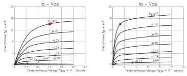
I bought qty=50 of the -7 suffix units, but haven't tested them. If real-life, real-world parts resemble the I-V curves in the datasheet, which they might or might not, then 2SK3557 offers a possibility of operating nicely at lower VDS.So what are your experiences with the 2SK3557
I put a red dot on the I-V curves from the 2SK3557 datasheet, showing where I might one day dare to operate the transistor in a circuit design: at VDS>=1.2 volts. The datasheet curves presumably display a "typical" unit. Perhaps if we somehow obtained an I-V curve of a plus-three-sigma "FAST" unit from the population of -7 suffix parts, its red dot might lie at, oh let's make a guess, VDS=1.7 volts.
_
Attachments
Last edited:
You mentioned "2SK3557 (Vdsmax=15V) are not that happy (noise wise) at Vds=4V"
So you must have measured them extensively, e.g. with different Vds ?
Can you show us some of your measurements ?
In the datasheet of the BF862, you can see how the gate leakage current changes with Vds.
No such info for the 2SK3557.
But in both cases, I think cascoding them at say 2~4V Vds is a good idea.
At least that is how we used to use them in the past (with a J111 as coscode).
Patrick
You mentioned "2SK3557 (Vdsmax=15V) are not that happy (noise wise) at Vds=4V"
So you must have measured them extensively, e.g. with different Vds ?
Can you show us some of your measurements ?
As I said, not me doing the skunk work, but I will ask and be back ASAP.
Borbely also stated that min operating voltage should be at least 2times Vpinchoff. He even showed a jig that measured Vpinchoff to allow the min operating voltage to be determined.Doesn't make much sense. Saturation onset is at Vds=|Vgs-Vp| and twice this value ensures a good saturation operating point. For devices working around Idss (Vgs=0) this is at 2 pinch voltages, that is not more than 2V (worst case). I've used BF862 at Vds=2.5V without any problem (noise or linearity wise).
Low noise jfets should be run at the lowest possible Vds, since otherwise there's a good chance to degrade the noise performance by hot carrier injection (from the reverse biased gate-drain junction) in the gate.
4V is probably not to bad for the BF862 anyway, but other devices like the 2SK3557 (Vdsmax=15V) are not that happy (noise wise) at Vds=4V, I can tell you that. Also in your post #18, it appears the "fast" DUT you are using as an example has a measured Vp well in excess of 1.2V (around 1.6-1.8V eyes only estimate) which is highly unusual and definitely outside the data sheet (Vp=1.2V max). Strange enough, since high Vp always leads to a lower transconductance (for a fixed device geometry, and barring any short channel effects).
BTW, why do you call those two BF862 classes you are using "slow" and "fast"?
The best-fit LTSPICE model parameters shown in post #1, are simply the numerical values that give the smallest fitting error (in the least-squares sense). They aren't measured values of "physical constants"; they're merely settings on simulator knobs.
Nevertheless ...
Suppose that, for some reason, we wanted an easy way to measure a BF862 and use that measurement to very quickly predict the simulation parameter "VTO" which would pop out of a long, time-consuming model fitting procedure. {For JFETs the LTSPICE parameter "VTO" roughly corresponds to "Pinchoff Voltage" except that subthreshold, impact ionization, and (3/2)-power effects are neglected}
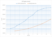
To find this out, I hooked up a couple power supplies and a couple 6.5 digit benchtop meters to the two Worst Case JFETs, and made a couple measurements.
This is not especially encouraging news; the drain currents @ VTO are not even close; they're a factor of 3 apart. Just as bad, the standard "Vp" test jig circuit e.g. Figure 5 of this article, with grounded gate and a resistor in the source leg, does not have one universal value of Rsource which reads VTO for the worst case BF862s. The required Rsource values differ by a factor of 5 (!). Bummer.
_
Nevertheless ...
Suppose that, for some reason, we wanted an easy way to measure a BF862 and use that measurement to very quickly predict the simulation parameter "VTO" which would pop out of a long, time-consuming model fitting procedure. {For JFETs the LTSPICE parameter "VTO" roughly corresponds to "Pinchoff Voltage" except that subthreshold, impact ionization, and (3/2)-power effects are neglected}
To find this out, I hooked up a couple power supplies and a couple 6.5 digit benchtop meters to the two Worst Case JFETs, and made a couple measurements.
Code:
Device       VGS(=VTO)   IDS     (V/I) ratio
---------------------------------------------
FAST BF862    -824 mV   12.3 uA     67 Kohms
SLOW BF862 -508 mV 37.8 uA 13 Kohms_
Attachments
Last edited:
More real life experiences, thanks.
Did you determine the Vp values Borbely-style and what were these?
In my batch I find -845mV for the Id(0)= 18.5mA one and -745mV for the device I measured at Id(0) = 14.5mA. Both Vp values taken with a DVM that has 1MOhm input resistance. Id I "measured" at 0.8uA.
I get higher values with a 10MOhm DVM, but these are dependent on how I look at the DUT, so I put them to one side.
More real life experiences, thanks.
I get higher values with a 10MOhm DVM, but these are dependent on how I look at the DUT, so I put them to one side.
If you include sub-threshold parameters Vp becomes somewhat meaningless, it gets bigger and bigger at lower and lower Id to the point where the value is useless in the model at normal Id. Just like using the level 1 model makes fussing about the details somewhat a waste of time, the low noise FET's everyone likes to use here have considerable short channel effects. In the level 3 model (Taki or Curtice) you can get the curves to lie almost exactly on reality over the entire Vds.
EDIT - someone posted this short but concise IEEE paper for free describing both problems. In their figure 2 the sqrt(Id) vs Vgs line should be straight and intersect the x axis at Vp. The correct Vp for normal applications should be interpolated from data in the quadratic region to the virtual intersection. You can't do much about the tanh() funtion in the Taki model and have to live with poor fit at lower Vds.
http://dlia.ir/Scientific/IEEE/iel1/16/2015/00055768.pdf
Last edited:
Thanks for the link, Scott.
Regards,
Patrick
Your welcome, most of my IEEE downloads are not for posting since we pay for them. One more thing LTSPICE does support the "B" parameter IIRC which allows a better fit if the device is not exactly square law. Simply take the data in the first region in the linked paper Vp is still the extrapolated intercept but if the slope is not 1/2 you can use the B parameter to fudge it. Someone should go through the exercise though I find the low noise FET's folks really worry about are very close to square law.
Last edited:
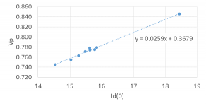
You probably all know this, but I see it the first time and I like how it looks ")
Id(0) - shown in mA - measured with +10V, a Drain resistor of 100 Ohms and Gate tied to ground. Vds thus varies with Id.
Vp - shown in V - is measured Borbely-style with 10V and a 1MOhm DVM btn Gate and Source.
Id(0) - shown in mA - measured with +10V, a Drain resistor of 100 Ohms and Gate tied to ground. Vds thus varies with Id.
Vp - shown in V - is measured Borbely-style with 10V and a 1MOhm DVM btn Gate and Source.
Attachments
Last edited:
As I said, not me doing the skunk work, but I will ask and be back ASAP.
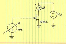
With permission from a former member here, the jfets gate current vs. drain-source voltage, at Id=Idss, measured with a Keithley 616 electrometer. The BF862 data points are, more or less, matching the data sheet.
Please recall that the gate noise current contribution per rtHz is SQRT(2*q*Ig). Also, as usual, paralleling devices increases the gate noise contribution by SQRT(N).
As you can see, the 2SK3557 gate current @Vds=4V is over two order of magnitude larger than the BF862.
My further comment:
- At Vds=4V, Inoise~18fA/rtHz.
- It takes a source resistance of about 20kohm or higher to have the gate current noise contribution relevant to the total noise budget (considering the channel voltage noise contribution 1nV/rtHz).
- 20kohm is a rather high source impedance in audio, but for a MM cartridge preamplifier it could matter, anyway BF862 could do much better.
- The 2SK3557 gate current contribution to the overall noise would be really critical for an electrostatic microphone preamplifier.
Attachments
The best-fit LTSPICE model parameters shown in post #1, are simply the numerical values that give the smallest fitting error (in the least-squares sense). They aren't measured values of "physical constants"; they're merely settings on simulator knobs.
Nevertheless ...
Suppose that, for some reason, we wanted an easy way to measure a BF862 and use that measurement to very quickly predict the simulation parameter "VTO" which would pop out of a long, time-consuming model fitting procedure. {For JFETs the LTSPICE parameter "VTO" roughly corresponds to "Pinchoff Voltage" except that subthreshold, impact ionization, and (3/2)-power effects are neglected}
To find this out, I hooked up a couple power supplies and a couple 6.5 digit benchtop meters to the two Worst Case JFETs, and made a couple measurements.
This is not especially encouraging news; the drain currents @ VTO are not even close; they're a factor of 3 apart. Just as bad, the standard "Vp" test jig circuit e.g. Figure 5 of this article, with grounded gate and a resistor in the source leg, does not have one universal value of Rsource which reads VTO for the worst case BF862s. The required Rsource values differ by a factor of 5 (!). Bummer.Code:Device VGS(=VTO) IDS (V/I) ratio --------------------------------------------- FAST BF862 -824 mV 12.3 uA 67 Kohms SLOW BF862 -508 mV 37.8 uA 13 Kohms
_
FWIW, to determine the pinch voltage, the usual recommended lab procedure is to measure Id vs. Vgs at a very small Vds (so in the jfet linear region), determine the linear region of the Id-Vgs curve (so make sure the subthreshold part is avoided, also avoiding high current effects, which are usually saturating the drain current at high Vgs) then extrapolate this linear region to Id=0.
Although this is not the usual datasheet definition of the pinch voltage, this method provides a good way to make an apple to apple comparison between devices. The same method applies to mosfets for determining the threshold voltage.
He says measure VTO at 1% of Idss.
Have you tried that?
It's just a convention, as good as any other (like measure Vgs at 100uA and call it the pinch voltage) which doesn't take into account the device-to-device different geometry, channel doping profiles, carrier mobility, etc... and makes device to device comparison error prone. Good as quick engineering estimate, though.
VTO is a number you feed into SPICE. Nobody "measures" VTO. Instead people curve-fit the SPICE equations to their measured I-V data, and then jiggle and twiddle with VTO to get maximum goodness-of-fit (minimum sum of squared errors).
Some people do try to measure "Vp", the pinchoff voltage of a real JFET that exhibits real subthreshold conduction, impact ionization, and non-squarelaw behavior. But the numbers they measure don't seem to correlate to the SPICE parameter VTO very well at all.
Maybe the whole idea is doomed and misguided: to search for shortcut ways to estimate VTO from one single measurement datapoint. Maybe the proper question to study is: what is the smallest necessary dataset? Or maybe, what is the easiest dataset to measure, which allows accurate extraction of VTO and the other SPICE model parameters? The easiest dataset might not necessarily be the smallest.
I invite you to combine the measurement data shown in post #27 with the other data shown in post #1, to test and explore the one percent theory of author "he" (whoever that is).
\
I invite you to combine the measurement data shown in post #27 with the other data shown in post #1, to test and explore the one percent theory of author "he" (whoever that is).
This is not a contest with winners and losers.
- Home
- Amplifiers
- Solid State
- LTSPICE models of worst-case BF862 JFETs