Perhaps the battery people will be able to tell you whether powering the Solid State Disk from its own super high quality voltage regulator (but not batteries), gives results as euphonic and pleasurable as when powering it from a battery. One presumes they tried a regulator before going all the way to batteries.
Understanding thermal data...
Hi. I'm trying to understand thermal characteristics more generally and the LM317 as a specific example. The datasheet for the LM317 provides:
Maximum power dissipation is a function of TJ(max), θJA, and TA. The maximum allowable power dissipation at any allowable ambient temperature is PD = (TJ(max) – TA)/θJA
For the TO-220 package TJ(max) = 150C and θJA = 19C/W (with a warning that operating at TJ(max) is unwise. So if I have an ambient temperature of 21C, the maximum power dissipation of the LM317 is 6.8 watts.
I understand that the power in watts that is dissipated as heat by a voltage regulator is the voltage drop multiplied by current. If this is correct and I have 12V input to a 5V regulator and up to 1.5A of current load I need to account for (up to) 10.5W of power dissipation and it will fail without heat sinking.
If I look at Mouser part number 532-529802B25G which is an Avid TO-220 heat sink, it has a thermal resistance of 3.7C/W. Does this mean that if this heatsink is coupled effectively to the LM317 that θJA becomes 3.7C/W instead of 19C/W? Does it mean that the temperature of the heat sink and LM317 will rise to circa 39 degrees Celsius above the ambient enclosure temperature for 12V input, 5V output and 1.5A?
Lastly, let's say we wanted to do an SMD version of this regulator with, for example, SOT-223 packages for the LM317 (or perhaps the LT3080). How does one manage such thermal issues?
Last edited:
Have you read the thermal modeling sections of Cordell's power amp book and Self's power amp book?
You'll need to include Theta-JC of the semiconductor, and also Theta-Case-Heatsink of the AttachmentDingus, and also Theta-Heatsink-Air of the heatsink, in your calculations.
"AttachmentDingus" might be (mica insulator plus thermal grease), or it might be (Kapton tape), or (T-gard insulation pad), or (Therafilm insulator), or (polyimide tape), or ...
Thanks. ") No I am struggling through the foregoing sections of Cordell's book first - I shall skip ahead to that section this evening.
No I am struggling through the foregoing sections of Cordell's book first - I shall skip ahead to that section this evening.
I was initially going to ask an even simpler question as to whether my understanding of the thermal resistance specification of a heat sink was correct. That is, do I read correctly that a thermal resistance of 3.7C/W means, quite simply, that the temperature of the heat sink will rise by 3.7C for every watt of power dissipated to it. (Lower is better.)
I then extended my question and invited a more complex answer - albeit I tried to make some simplifying assumptions. (That'll teach me.) I recognise that the heat transferability of the "AttachmentDingus" is a factor in any precise calculations and so I cheated by saying "coupled effectively" (by which I meant perfect transfer) to add a significant degree of simplification to my question. I also presume that, when considering a semiconductor coupled to a heat sink, θJC and θAD are more relevant than θJA but in my example and with my simplifying assumption the two are roughly the same. Isn't Theta-Heat Sink-Air embodied in the measure of it's thermal resistance? And so back to my initial question...
Thx for the guidance
No I am struggling through the foregoing sections of Cordell's book first - I shall skip ahead to that section this evening. I was initially going to ask an even simpler question as to whether my understanding of the thermal resistance specification of a heat sink was correct. That is, do I read correctly that a thermal resistance of 3.7C/W means, quite simply, that the temperature of the heat sink will rise by 3.7C for every watt of power dissipated to it. (Lower is better.)
I then extended my question and invited a more complex answer - albeit I tried to make some simplifying assumptions. (That'll teach me.) I recognise that the heat transferability of the "AttachmentDingus" is a factor in any precise calculations and so I cheated by saying "coupled effectively" (by which I meant perfect transfer) to add a significant degree of simplification to my question. I also presume that, when considering a semiconductor coupled to a heat sink, θJC and θAD are more relevant than θJA but in my example and with my simplifying assumption the two are roughly the same. Isn't Theta-Heat Sink-Air embodied in the measure of it's thermal resistance? And so back to my initial question...
Thx for the guidance
theta_ja = theta_jc + theta_ca. The point is theta_dingus + theta_sink_a is quite a bit less than theta_ca. Your question about 3.7 C/W is correct to a zero order approximation. But be aware theta_sink_a varies as a function of the temperature rise in the heat sink. That needs to be accounted for when operating the heat sink away from its specified Trise.
Thanks guys.
Well I have this little regulator up and running on a bread board - the first thing I have ever bread-boarded. I'm glad it actually works. I was trying to look at the noise on my new scope but it seems to pick up a lot more than I expected. I suspect that's in good part due to all the jumper wiring. (I need to find some good tutorials on how to use my scope properly.)
I also picked up a couple of errors in my Eagle PCB work. (I had been so focused on the 243R resistors that I completely forgot to check the size of the 8.2K one which is obviously significantly bigger. Plus I had the SPX431 around the wrong way - it could be rotated 180 degrees easily enough but would be counter to the silk depiction. The package also differed from the data sheet in that the pins are already splayed further apart than depicted in the data sheet - I had spaced the holes thinking I would have to bend the pins some but in fact they are already splayed further than the holes I had created.
All 'n all, a good learning exercise thus far.
SGK: yep, your understanding is basically right. Thermal resistances behave just like electrical resistances with the following equivalence:
- thermal resistance (K/W) is resistance
- power flow (W) is current
- temperature (K) is voltage
- fixed temps, e.g. ambient, are voltage sources
- thermal mass (K/J = K/W-s) is capacitance
If you're comfortable analysing a simple resistive circuit, you can draw out an equivalent circuit with resistors for thermal resistances, current sources for thermal sources, capacitor for thermal masses, etc. If you care only about steady-state performance then just leave the capacitors out entirely.
So your TO220 dissipating 10.5W is a 10.5A current source, and it has a 19 ohm theta_ja in series. That's connected to ambient (a 25C voltage source, usually one uses 40C for conservatism), which connects to ground. That means that the junction is at 200C above ambient, and it will melt unless you're using it with an ambient temp of -50C or lower...
When you add a heatsink, you're effectively splitting the device's theta_ja into two series resistors, theta_jc+theta_ca as twest says. You now put the (hopefully very small) heatsink resistance theta_hs = theta_dingus+theta_heatsink_specification in parallel with the (typically large) theta_ca:
theta_ja = theta_jc + 1/(1/theta_ca + 1/theta_hs)
and since theta_jc is pretty small, your total resistance is now small and the junction temperature is nice and low. And since theta_ca is so big compared to theta_hs, you can conservatively ignore it and gain some simplicity:
theta_ja = theta_jc + theta_hs = theta_jc + theta_dingus + theta_heatsink_specification
Fret not about PCB errors. It takes some experience - actually manufacturing a several different designs - before you get to the point where you've made a good fraction of the possible errors.
Last edited:
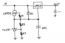
I try LM317 with TL431 from adj pin to ground, and jfet ccs from out pin to adj (set to 10mA).
Feedback network is 10k+2k, so i get something like 15V output.
No cap in the feedback network, no cap as compensation in TL431.
The circuit oscillates at 7MHz without output cap and with any load over 100mA current. Without load the circuit doesn't oscillate.
I add a Panasonic FM 220uF 16V at output (100mohm ESR) and now the circuit is dead quiet up to 1.5A.
Can't see any ripple/noise over the EMI noise from my ambient (electronic's lab).
DO NOT use cap in feedback network: it improves PSRR but transient response is sloooow as hell.
I try to increase output capacitor and the circuit is stable even with 4700uF and 10mohm ESR.
So..
- The circuit requires a light amount of output capacitance or will oscillate with load (not at idle). It's stable with high output capacitances.
- The circuit doesn't need any cap in feedback network or compensation.
- The circuit works also without input capacitance.
The results are:
- improved PSRR (simulation shows LMpsrr+TLgain...like 120dB total in audio band)...cannot measure such huge rejection with my instrumentation.
- improved transient response (faster and less over/undershoot)
The only difference from LTspice sims and real life it's the oscillation without any cap at output: LTspice shows no problem, real life yes.
Last edited:
I ran with this in the end although with the TL431 replaced by an Exar SPX431AN. Any comments? Drop C2?
An externally hosted image should be here but it was not working when we last tested it.
C2 must be removed if you want fast transient response (for example if your Vout have to deliver variable current)
You can bias the TL431 with R1 from cathode to Vout (of LM317), so the bias will be more stable. I replace it with a n-jfet as CCS (i also try an LM334 set for 8mA) for more costant bias with great results.
You can bias the TL431 with R1 from cathode to Vout (of LM317), so the bias will be more stable. I replace it with a n-jfet as CCS (i also try an LM334 set for 8mA) for more costant bias with great results.
No. The first posts in this thread discuss (a) stabilizing the amplifier cascade that results from attaching a TL431 to an LM317's "ADJ" pin; and (b) the noise implications of different stabilization mechanisms (capacitor placements).I thought the conclusion from the discussion in the first few pages of this thread was NOT to shift R1 from Vin of LM317 to Vout of LM317...
Whether you choose to bias the TL431's cathode from Vin or from Vout, in either case you still have the option of (a) using a current source: JFET or LM334 {post 51}; (b) using two resistors and one BFC {post#13} .
Ok. Let me know if any of this is wrong. (If there are more accurate ways of expressing things please feel free to comment also.)
If one removes C2 from the circuit I posted you basically get the circuit published in the application note for the TL431, the only addition is a 0.1uF bypass cap recommended in the LM317 datasheet and a 470uF output cap. The voltage divider R2 and R3 sets the reference voltage for the circuit. The addition of the TL431 to the more basic typical LM317 circuit is there to improve the stability of Vadj. (The LM317 “rides” on a more stable reference voltage.) A drawback of providing current for the TL431 (or SPX431) via R1 from Vin is that this bias is susceptible to fluctuations in Vin.
The initial proposal was to simply shift the bias from Vin to Vout, but the OP, having heard from twest820 in post #11, decided to keep it out of the feedback loop (although I inferred that C1 in his case, C2 in mine, remained). I profess to not yet understanding even the basics of “open loop gain”. Later, post #28, it was recommended for me to stick with the input version as simpler and safer. (The other suggestion to place a cap between cathode and Vref of the TL431 didn’t, to me at least, pan out.)
As Mark notes, in post #13 he suggested an easy improvement to the circuit which would be applicable regardless of whether one took the Vin or Vout approach. I certainly missed this suggestion. I am unsure that I understand why it improves things and an explanation would be greatly appreciated (as well as an explanation for the abbreviation BFC). I am going to guess and say that it creates a low pass filter with the cap set such that the break frequency (1/RC in radians) is below 50Hz. (BFC = break frequency cap?) Hence the impact of mains cycle ripple on the bias current is diminished.
Alternatively, as Pergo pointed out, Mark reminds and as I read last night in 2.05 of The Art of Electronics, the circuit could be improved by provided the bias from a current source (CCS = current source, I presume). Pergo, can you post your suggested circuit? (JFET or LM334 sits between LM317 out and LM317 adj I presume.)
How do you guys look at oscillation? Same with transients? I had thought that transients would be borne first and foremost by the output cap.
Am I learning/making progress?
I've built this in a breadboard:
Output cap is Panasonic FM. Jfet had Idss > 5mA (12mA in my case).
The circuit is stable at any load (up to 1.5A current).
Simulation shows improved transient response.
I will try to measure it.
Output noise and ripple is below ambient pickup noise (my lab is full of EMI)
TL431 and LM317 are from Fairchild.
An externally hosted image should be here but it was not working when we last tested it.
Output cap is Panasonic FM. Jfet had Idss > 5mA (12mA in my case).
The circuit is stable at any load (up to 1.5A current).
Simulation shows improved transient response.
I will try to measure it.
Output noise and ripple is below ambient pickup noise (my lab is full of EMI)
TL431 and LM317 are from Fairchild.
For those who don't want to worry about the stability of cascaded amplifiers, the input-biased variant may be pleasing. Especially in applications like a 12VDC input, 5VDC output regulator which powers a solid state disk. The 12VDC input won't have nearly as much ripple as the standard (trafo + rectifier + capacitor).
BFC is a Large Capacitor, at least 33uF {see red dot}. It keeps the TL431 delightfully stable, it shunts noise to ground, and it keeps the impedance low at the ADJ pin, even at high frequencies.
R1 is about 8.2 ohms, which sets the LM334 current source IC to deliver 8 milliamps.
The (R2/R3) ratio is chosen to be 0.50; therefore the TL431 cathode voltage is ((1 + 0.5) x 2.50) = 3.75 volts. This is applied to the LM317's ADJ pin, producing an output of 5.00 volts. {R2 = 1K2 and R3 = 2K4 would be reasonable choices}
D1 protects the LM317 if the input gets shorted to ground. When this happens, BFC is discharged through D1 instead of through the sensitive ADJ circuitry inside the LM317. I would select a low capacitance diode (based on datasheet MAX Cj@0V, not datasheet typical) like the 1N4149 in this position.
Attachments
Last edited:
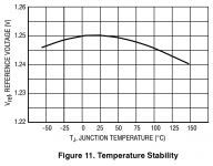
You are aware that the TL431 will drift with temperature?
4-25mV in Vref over -40 to +150°C, so in my case 24-150mV for 15V output.
Something like <1mV/°C.
4-25mV in Vref over -40 to +150°C, so in my case 24-150mV for 15V output.
The LM317's internal Vref varies about 10mV over temperature, so the barebones 317 circuit without the TL431 drifts (15.0/1.25)x10mV = 120mV for 15V output. 120 isn't a whole lot better than 150 millivolts.
Attachments
- Status
- This old topic is closed. If you want to reopen this topic, contact a moderator using the "Report Post" button.
- Home
- Amplifiers
- Power Supplies
- LM317+TL431, really?