I should've tested them before mounting them. None of the legs are shorted with the heat sinks however. Just baffling. I'm not sure which particular resistor got hot. What's next? Thanks David.
I bought one unassembled and after mounting to a heatsink I used a multi meter set to short test and tested all transistor legs to heat sink to make sure there was no contact.
Are all the transistors getting hot at the same time or just one?
Before assembly I tested every transistor to make sure none were duds.
L20V9
I posted another reply but it got lost in the ether. Let's hope this one works. The output transistors are not mosfets or weren't on my boards. They are PNP/NPN. make sure the correct types are in the correct holes. Look up the specs on the net. The small transistor on the heatsink had exposed metal on its mounting surface on my boards so I put a silicon washer under it. I don't see a washer under yours but if you have checked the legs to ground I guess it's OK. The drivers were mosfets on my boards (?610/?9610). The small transistor on the heatsink was an ?669 bipolar. Don't take all this as gospel as your boards might be different. If you have fried some of the output transistors you can still use the board at lower power with a pair of transistors instead of the full 4 pairs. I did that whilst I was waiting for replacements. I would not worry about fiddling with the bias at this stage as it should be in the ball park if the resistor values are OK. If any of the resistors got hot it will probably be some of the 0.22ohm ceramic emitter resistors. Make sure they are not open circuit now.
I posted another reply but it got lost in the ether. Let's hope this one works. The output transistors are not mosfets or weren't on my boards. They are PNP/NPN. make sure the correct types are in the correct holes. Look up the specs on the net. The small transistor on the heatsink had exposed metal on its mounting surface on my boards so I put a silicon washer under it. I don't see a washer under yours but if you have checked the legs to ground I guess it's OK. The drivers were mosfets on my boards (?610/?9610). The small transistor on the heatsink was an ?669 bipolar. Don't take all this as gospel as your boards might be different. If you have fried some of the output transistors you can still use the board at lower power with a pair of transistors instead of the full 4 pairs. I did that whilst I was waiting for replacements. I would not worry about fiddling with the bias at this stage as it should be in the ball park if the resistor values are OK. If any of the resistors got hot it will probably be some of the 0.22ohm ceramic emitter resistors. Make sure they are not open circuit now.
David,
The two boards are assembled exactly the same way. I went over all the soldering spots with a magnifying glass to make sure I don't have loose joints or overlapping joints. All the transistors are installed with insulators between the heat sink and the exposed metal parts, and continuity testing validate that they don't touch. The 669 transistor is the only part that does not have exposed metal. And yes, the PNPs and NPNs are in the correct positions. How do I know that? One channel works fine, the other turns real hot.
The two boards are assembled exactly the same way. I went over all the soldering spots with a magnifying glass to make sure I don't have loose joints or overlapping joints. All the transistors are installed with insulators between the heat sink and the exposed metal parts, and continuity testing validate that they don't touch. The 669 transistor is the only part that does not have exposed metal. And yes, the PNPs and NPNs are in the correct positions. How do I know that? One channel works fine, the other turns real hot.
I posted another reply but it got lost in the ether. Let's hope this one works. The output transistors are not mosfets or weren't on my boards. They are PNP/NPN. make sure the correct types are in the correct holes. Look up the specs on the net. The small transistor on the heatsink had exposed metal on its mounting surface on my boards so I put a silicon washer under it. I don't see a washer under yours but if you have checked the legs to ground I guess it's OK. The drivers were mosfets on my boards (?610/?9610). The small transistor on the heatsink was an ?669 bipolar. Don't take all this as gospel as your boards might be different. If you have fried some of the output transistors you can still use the board at lower power with a pair of transistors instead of the full 4 pairs. I did that whilst I was waiting for replacements. I would not worry about fiddling with the bias at this stage as it should be in the ball park if the resistor values are OK. If any of the resistors got hot it will probably be some of the 0.22ohm ceramic emitter resistors. Make sure they are not open circuit now.
The other thing I'd like to point out to all is that ljm_ljm has been completely silent over these issues. He also did not reply to my emails to him. I'll just let you draw your own conclusions, but instead of advertising newer products, I think he should be addressing issues with existing ones. On my part, live and learn.
Your board is exhibiting the same problems as a couple of pre-built boards I purchased. I couldn't pin down the actual cause but suspected it was very high frequency feedback possibly due to the rats nest I had cobbled up to get them going. Some of the output transistors went short circuit as a result. Later when I had made the wiring a bit neater and replaced the transistors the problem went away. I suggest you only install one pair of good output transistors when you next try the faulty amp. Temporary 1 amp fuses in the +/- rails would also be a good idea. As for ljm...he is obviously a lot smarter than I am but his English is like my Chinese, and he really should get someone to write his responses so that they can be understood. There are some very early posts on these amps with some useful info and they might be worth chasing up. There was a 200 ohm 1W resistor between the two mosfets (610/9610) on my boards and the voltage across this resistor develops the bias voltage for the output pairs. Maybe you could compare the voltage on the two boards. I think (and I may be wrong) that with the output devices removed you can still measure this voltage and it would be around 1.4 to 1.6VDC. Maybe someone could comment on this.
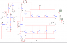
Schematic for V7
Hi all!
This is the schematic for L20VER7, I re-engineered from a PCB.
It looks plausible to me. (R13 originally was 1k1, what biased the output-trannies to 450mA! in idle. I went for 100mA bias -> 2k2)
It seems, that B and C of T21(2N5551) are swapped.
If the transistor would be installed, as indicated on the PCB, there might be problem.
I haven't assemled the kit yet.
THD was 0.02% (2Vpp in, 4Ohm, 384W out, 1 kHz) and 0.006% (1Vpp in, 4Ohm, 86W out, 1 kHz) in simulation. THD20 was much more.
However, this chinese stuff is cheap.
Cheers,
Peter H.
Attachments
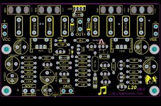
L20
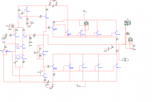
In the attachment, there is a schematic, I found in the internet - or may be here in the forum. I don't know whether it's correct.
Is it noise or hum?
In case of noise:
You coud try 100n (or more) parallel to B and E of Q6.
100n parallel to R25 might help, too.
Try without R7 and C3. IMO this adds distortion.
However, the transistors are no low noise types, since they are not available at these high voltages.
VER7 is also quite noisy.
How is the amp biased? 100mA should be appropriate. There should be 22mV on the resistors R29, 30 etc.
Which supply voltage do you measure in idle?
Attachments
This is not the correct circuit.In the attachment, there is a schematic, I found in the internet - or may be here in the forum. I don't know whether it's correct.
Is it noise or hum?
In case of noise:
You coud try 100n (or more) parallel to B and E of Q6.
100n parallel to R25 might help, too.
Try without R7 and C3. IMO this adds distortion.
However, the transistors are no low noise types, since they are not available at these high voltages.
VER7 is also quite noisy.
How is the amp biased? 100mA should be appropriate. There should be 22mV on the resistors R29, 30 etc.
Which supply voltage do you measure in idle?
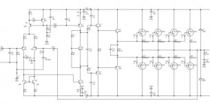
L20 noise is very low.
..i guess not,,it would help to see that low noise stage
Noise will not change because of the transistor.
Noise is PCB circuit.
L20 is stable. There would be no oscillation.
L20 Use the CFP input structure. Input stage distortion and noise is very low.
Even can ignore its existence.
Attachments
Guys,
Don't even try this. My L20s ran fine with +/-56V, and smoked when I put them on +/-68V. It also depends on the load, but stay away from high voltages.
Don't even try this. My L20s ran fine with +/-56V, and smoked when I put them on +/-68V. It also depends on the load, but stay away from high voltages.
VER7 VER9 + -70V OK.
This is likely - the power transistors are rated 140V breakdown voltage. This cannot work.
Finally, I decided to use an own design, based on the 'high side' of a Crown MA-600.
It can drive 2 Ohms, has some protection features and the simulation shows THD20 of 0.0003 almost independent from output power.
May be, I use the L20 kits for an other project.
Finally, I decided to use an own design, based on the 'high side' of a Crown MA-600.
It can drive 2 Ohms, has some protection features and the simulation shows THD20 of 0.0003 almost independent from output power.
May be, I use the L20 kits for an other project.
- Home
- Amplifiers
- Solid State
- L20 V8