PH104 said:John -- What voltage gain stage are you using for your amp? I've seen something similar too, and always on the negative half of the square wave.
I'm driving the output stage only from my function generator. Whatever this is, it is in the OS. It was there in my point to point version as well. Same deal - the negative half.
PH104 said:John
what load are you using?
I'm using an 8 ohm dummy
Of course but not before tonight!Andypairo said:Nice one Boraomega, can you also provide
a matching schematic?
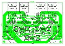
Which software did you use?
I am using TSIEN Board Maker from "Jurasic period"!

")
Well, I gave my best to do that sooner...
I intentionally omitted components values and people should use those proposed by Steve. With given arrangement of four diodes and trim pot, bias adjustment should be more flexible because it is possible to set trimmer short which will leave only two diodes in action (other two will be shorted by trimmer) or all four diodes will contribute when trimmer is at maximal resistance therefore covering continually all cases between "having two" to "having four" diodes. I used two small transistors 2SC2240 & 2SA970 instead of bigger ones originally proposed, because their dissipation is never more than a few tens of mW and they are with much better gain making regulation more dynamic.
I have to highlight: I haven't tried this circuit in practice, but I believe it will work nicely.
Attachments
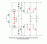
originally posted by boraomega
I used two small transistors 2SC2240 & 2SA970 instead of bigger ones originally proposed, because their dissipation is never more than a few tens of mW and they are with much better gain making regulation more dynamic.
boraomega -- thanks for pointing this out. I've been looking at other transistors for the bias and input pair and never stopped to think about the power dissipation for the bias transistors. Duh...........
I'm going to try the 2SA1210/2SC2912 pair today. I want to be able to screw them down on the main heatsink.
At +- 50 V....
The input pair dissipates app 550 mW
The bias pair..dissipates app 3-5 mW
The predrivers app 500 mW
I can't figure out how much the bias pair contrubutes to the thermal compensaton...Signal wise the two input pairs does nothing......Or so it seems to me..
I have tried to simulate a circuit omitting thesse two transistor pais.. and got just as good results....Still with the non switcing element intact...
hmmm
boraomega said:
I have to highlight: I haven't tried this circuit in practice, but I believe it will work nicely.
It will work.
Steve Dunlap said:
I have received E-mails from several builders that have successfully built the amp already. They are pleased with the performance and even (if this is relevant), the sound. There have been reports of slight overshoot on the leading edge of square waves above 100KHz. I will have to work on that.
scott wurcer said:How long are we going to carry on this charade?
http://www.diyaudio.com/forums/showthread.php?postid=1814524#post1814524

MJL21193 said:Looks good Steve.
My compliments to Thomas for getting it together.
Thank U John
Steve – I sincerely regret having used such harsh words over such a trivial technical point. At the time I was honestly convinced that there was mischief or financial matters involved.
Let me reduce the contradiction to as simple a case as I can. Just quasi-DC or low frequency, the full power sine/square wave stuff at 10k and above just serves to obscure things. The point was made several times that “the voltage between the bases does not change with signal”. Sorry I don’t have the time to find the exact quote. Reduce it again to just a complimentary follower and .22 Ohm emitter ballast. Say, for arguments sake, that the NPN and PNP both have the same Vbe of 700mV at 30mA, between the bases that would be 1.4132V. Now source 3A. That, roughly, is 100X the current or about 120mV increase in Vbe (820mV) and .66V across the top .22 Ohm resistor or 1.48V. With no change in the voltage between the bases that leaves -66.8 across the other device. Your devices had 575mV Vbe’s but that does not change the result (actually makes it worse). To operate the upper device at 3A and (to be generous) keep the lower one on at just say 1uA would require ~1.913V across the bases. Things vary with temperature but the point seems to keep everything at the same temperature so this is also an unnecessary complication.
This has nothing to do with models, simulators, or beta for that matter. Sliding bias schemes exist, but they all adjust the voltages to keep the device in the forward active region. There are even ones that use geometric mean (constant product) biasing. BTW I don’t really care about switching/non-switching behavior, in open loop circuits full power response tests bury small things that go on at crossover.
Hi Scott,
A valid example. That does make it sound like I am incorrect. However, when the base to emitter voltage on the output stage of my amp is measured, it does increase. This led me to believe the transistors might not be turning completely off. Well, that and the fact that current can be measured in the collector throughout the signal.
It has been some time since I made those measurements. It is possible that the 4 near death experiences I have had since then have affected my memory. In case someone plans to ask, there was no light, at least not for me.
Steve Dunlap said:However, when the base to emitter voltage on the output stage of my amp is measured, it does increase.
Simulation shows that too. This initially surprised the heck out of me. It happens because the driver Vbe gets reverse biased, thus increasing the voltage difference between the output stage bases relative to the quiescent condition. The driver turns off abruptly, leaving no path for the stored base charge in the output devices to be swept out. So the output stage Vbe's remain forward biased for a time, but eventually they turn off - but rather slowly.
andy_c said:
Simulation shows that too. This initially surprised the heck out of me. It happens because the driver Vbe gets reverse biased, thus increasing the voltage difference between the output stage bases relative to the quiescent condition. The driver turns off abruptly, leaving no path for the stored base charge in the output devices to be swept out. So the output stage Vbe's remain forward biased for a time, but eventually they turn off - but rather slowly.
Could this be the reason the distortion goes down at higher frequencies? This would explain some of what I remember measuring.
scott wurcer said:That's why I wanted to talk DC, the explaination's offered walked through the schematic in a DC fashion. I wanted to separate switching behavior from simple voltage transfer non-linearity.
It never occurred to me to do DC measurements on an audio amp. At DC you may be correct. My simulations do show current flowing in the collectors of the outputs with a DC input. My simulation could be flawed.
Just curious, how much switching distortion do the transistors produce at DC?
- Status
- This old topic is closed. If you want to reopen this topic, contact a moderator using the "Report Post" button.
- Home
- Amplifiers
- Solid State
- Krill - The little amp that might...