apassgear said:
Much has been said but it would be nice to hear some tips on how a good layout should be done to avoid certain pitfalls. For example, how to lay a hi impedance node to avoid interaction? Under a ground plane? Surrounded by power supply rails?
With all the experience around this thread we might get some good praxis.
Actually it's an interesting topic... and a question is always a good place to start a conversation from.
My take on laying out any high impedance node is to keep it a small as possible (duh!), which means the layout starts by arranging all of your gain devices to accomplish this. Any attempt to shield or bypass these nodes with planes or to the power supplies is misguided.
Look at the various loops involved in an operating gain stage, separate the supply and biasing currents from the signal loop and it's reference, you'll see the signal has very little relationship to these currents. Placing the signals anywhere near them just tends to force a reaction that is in any form a negative effect.
Regards, Mike.
anatech said:Hi Mike,
You can place a guard around this point and drive it with a buffered version of that signal so that there is no voltage gradient near your sensitive circuit.
Not always possible to do, but worth it if you can.
-Chris
I've read about this but have never tried it. I just try to arrange things so it's less of a problem.
Another poster noted that we are not dealing with the technical fringe here, and I agree with him that (signal wise) we are only dealing with what a 1950's benchmark was able to produce remarkably spooky results with, regardless of the limited bandwidth.
Goodnight, Mike.
john curl said:
Of course, in 1974, I originally thought that my Levinson JC-2 was PERFECT!
I was convinced my first compact stereo was perfect. (A long pause whilst the laughter dies down...) It took more years than I care to contemplate for me to learn that there was more. It was a long climb out of the morass--unfortunately lengthened by a detour into the specs-are-everything jungle. I guess that was just my kharma working on me...musta done somebody wrong in a previous incarnation or something. Since then I've made fairly steady progress in getting where I want to be.
The interesting thing is that I (like John, like Nelson, like Charles) learned that less is more.
Grey
Guarding and shielded guarding are really the most powerful techniques to keep high-Z nets clean (or to isolate any nets sensivite to stray capacitance). One only has to take care that a buffer driving the guard with the AC signal copy doesn't introduce more problems than it tries to solve. The buffer input loads the signal, and stability problems can arise, especially when the buffer drives a cable shield as a guard. Usually one has a buffered/amplified copy of the signal (or only a linear distorted copy, that is with some minimum phase filtering) lying around anyway, and from that one can derive the low-Z guard drive, thus no extra buffer, directly and additionally loading the signal, may be needed.
One might explore the AppNote sections of Analog Devices, National Semiconductor, Linear Technologies and many other semicon companies. Plus some books, like Henry Ott's classic "Noise Reduction Techniques in Electronic Systems" and especially the Keathley "Low Level Measurements Handbook".
Which boils down, layout-wise (like Mike and Chris have pointed out): Keep the net's surface area small and stay away at least 1/4" from anything which isn't more or less an exact AC copy of the signal itself. These "no gos" include ground (planes) and psu signals. And if you need to get close to other signals, choose the ones which are closest to clean AC-ground potential (supply lines don't need apply, usually).
For an amp this means you may be able to guard the sensitive nets with an output or interstage signal, probably divided down to the same AC level with resistor dividers (which can be trimmed with C shunts for maximum perfomance, or filtered with the inverse of any minimum phase filter in the signal chain, to restore the original signal waveform). Of course with the same polarity (therefore one might need an inverter). Even if the guard potential is not an exact copy it will help the signal to stay clean very much. Only the difference between signal and guard is the effective voltage any capacitance (and it nonlinearities) can work upon. The guard should envelope the net as much as possible, which also assist local shielding.
- Klaus
KSTR said:One might explore the AppNote sections of Analog Devices, National Semiconductor, Linear Technologies and many other semicon companies. Plus some books, like Henry Ott's classic "Noise Reduction Techniques in Electronic Systems" and especially the Keathley "Low Level Measurements Handbook".
A short list of my reference library on the subject. Grounding and Shielding Techniques in Instrumentation By Ralph Morrison should be incuded in anyones list.
apassgear said:And now on a practical mood, if someone cares to comment. No fear…
Much has been said but it would be nice to hear some tips on how a good layout should be done to avoid certain pitfalls.
KSTR said:Guarding and shielded guarding are really the most powerful techniques to keep high-Z nets clean.
- Klaus
The application of guarding is on a much higher level than the DIY-fer trying to build a circuit to see what it sounds like. Practically it can really only be used to protect the signal coming into a functional block or in the type of applications that Klaus works with. Applying it to all Hi-Z nets in an audio application would be a nightmare, even if you could control all of the variables.
My approach is to highlight all of the sensitive nets on the schematic and to use this as a guide for placing the components. I keep the +/- supplies as straight shots down either side of the stage, with ground running below (if possible) and try to arrange the placement of signal ground leads to a common point, not snaked around. I also identify all of the functional loops and try to keep them as small as possible. Most Hi-Z nets have very low currents so you can minimize the effect of the DA by keeping their footprint small. Also use the exact footprints of the parts you are going to use, as there is no cheating the space God once the board is made.
This is a simplification, but once you have all the components on the screen and start to try different scenarious it can become quite interesting. I find my self analyzing moves and their effect in the same way you would play a game; all based on the knowlege gained through the various books listed earlier and experience.
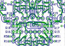
I've attached a screen shot of part of the signal layer of a MC amp I'm laying out. It did not start out anywhere near this compact and I was quite pleased when things fell into place. I wanted to use the same PCB/powersupply layout as an IC based earlier design, but I doubted I could make the discrete design fit on the same board.
Regards, Mike.
Attachments
MikeBettinger said:
My approach is to highlight all of the sensitive nets on the schematic and to use this as a guide for placing the components. I keep the +/- supplies as straight shots down either side of the stage, with ground running below (if possible) and try to arrange the placement of signal ground leads to a common point, not snaked around. I also identify all of the functional loops and try to keep them as small as possible. Most Hi-Z nets have very low currents so you can minimize the effect of the DA by keeping their footprint small. Also use the exact footprints of the parts you are going to use, as there is no cheating the space God once the board is made.
This is a simplification, but once you have all the components on the screen and start to try different scenarious it can become quite interesting. I find my self analyzing moves and their effect in the same way you would play a game; all based on the knowlege gained through the various books listed earlier and experience.
I've attached a screen shot of part of the signal layer of a MC amp I'm laying out. It did not start out anywhere near this compact and I was quite pleased when things fell into place. I wanted to use the same PCB/powersupply layout as an IC based earlier design, but I doubted I could make the discrete design fit on the same board.
Regards, Mike.
Mike,
This is a great post; I appreciate for all the tips and information you give showing the way to proceed.
Hope others will share their experience too

P.S. I also appreciate Klaus contribution, thanks. There are great guys on this forum who share good information.
This (and trying to seperate the current loops) is IMHO of greatest importance, much more influence on quality than the capacitance/DA stuff. And the more power/current involved, the more so... my "trick" to do this is NOT to use any GND or PSU shortcut symbols in the schematic (and I learned that from old tube circuit schematics, BTW). I really have to admit that it took me some 15 years to actually obey to the simple rule that currents flow in loops and one needs the "think-in-current-loops"-approach to get it right, rather than "think-in-voltages" (which is more intuitive, though). I had to learn it the hard way, with quite a few of SMPS layouts that failed (EMC tests and also desired perfomance).MikeBettinger said:I also identify all of the functional loops and try to keep them as small as possible.
- Klaus
KSTR said:This (and trying to seperate the current loops) is IMHO of greatest importance, much more influence on quality than the capacitance/DA stuff. And the more power/current involved, the more so... my "trick" to do this is NOT to use any GND or PSU shortcut symbols in the schematic (and I learned that from old tube circuit schematics, BTW). I really have to admit that it took me some 15 years to actually obey to the simple rule that currents flow in loops and one needs the "think-in-current-loops"-approach to get it right, rather than "think-in-voltages" (which is more intuitive, though). I had to learn it the hard way, with quite a few of SMPS layouts that failed (EMC tests and also desired perfomance).
- Klaus
That’s very useful information; you make me remember seeing the welding electrode cables from an arc welder laying on the floor of a shop gathering around all the ferrous debris from about 4 inches away.
apassgear said:Mike,
Two questions, do you use standing regular resistors on a tight layout as the one you show?
Which is your favorite resistor for this type of application?
Actually I haven't used standing resistors in years. I regularly populate parts on both sides to help a layout, but was struggling with this layout and stood a couple up and it really helped. It kind took on a life of it's own from there. The power supplies on either side of the audio circuitry are a more conventional layout, mostly because I didn't want to change to much from the IC based design I want to compare this to.
I've built with all of the audiophile certified good parts over the years but on my past couple of projects I've been using Dale metal films. Good performance, range of values and availible.
Mike.
KSTR said:my "trick" to do this is NOT to use any GND or PSU shortcut symbols in the schematic (and I learned that from old tube circuit schematics, BTW). - Klaus
Interesting to hear someone else thinking along these lines.
Mike.
For sure!I really have to admit that it took me some 15 years to actually obey to the simple rule that currents flow in loops and one needs the "think-in-current-loops"-approach to get it right, rather than "think-in-voltages" (which is more intuitive, though).
You can then mentally recognize each wire as a low value resistor and inductor. I also try to keep the signal flow as reasonably short as I can. This can be compatible with the loop idea.
One of the problems for older members is that we were taught to think voltages as a primary thing, rather than the result of current flow. This is okay for very low current stuff (= high impedance), but a disaster when it comes to a heater supply for example. Solid state amplifiers are all about current flow. It can be hard to switch your thinking back and forth.
I like the idea of identifying the high impedance points on a schematic. We do this on an unconscious level, but it's helpful to force the idea.
-Chris
Hi,
Agree, interesting subject!
It took me some years to se this to.
Usually great care is taken by twisting supply wires etc. But sometimes it seems like RCL seas to exist when "wires" are placed on a PCB.
Look at well designed commercial stuff; usually these issues are well taken care of.
Agree, interesting subject!
It took me some years to se this to.
Usually great care is taken by twisting supply wires etc. But sometimes it seems like RCL seas to exist when "wires" are placed on a PCB.
Look at well designed commercial stuff; usually these issues are well taken care of.
Once in a while, I still use stand up resistors. Usually, when I just can't afford to make a crossover and space is limited. With 1/4W resistors, it has worked out OK, but larger might be a problem. This is because the return path of one side of the resistor is necessarily longer than optimum. I usually put the extra lead length in a teflon tube, to keep it out of the air as much as possible.
john curl said:Once in a while, I still use stand up resistors. Usually, when I just can't afford to make a crossover and space is limited. With 1/4W resistors, it has worked out OK, but larger might be a problem. This is because the return path of one side of the resistor is necessarily longer than optimum. I usually put the extra lead length in a teflon tube, to keep it out of the air as much as possible.
Hi John,
I oriented the longer leads to either the supply or the lower impedance nodes. I'm hoping there aren't any problems caused by standing them up, but I'm guessing not... It does make for a very compact layout.
The teflon tube is a good idea. It will make it look a bit better as well.
Also one general note: I realize the part numbers for the Fets in the image I posted are located over the pads, which one would not normally want to do as it messes with the solderability and printing over a hole doesn't generally work well
. I placed them there to allow me to print out a stuffing guide for assembly and I'll be having the boards made without silkscreening. As compact as the layout is I wouldn't be able to read it anyway.Another personal tip for consideration: I place my power busses and ground nodes on the top layer and my signal traces on the bottom; ground returns under power busses.. If the boards are mounted horizontally there is less of a problem with dust and airbourne contamination causing leakage between the more sensitive traces on the bottom side. It's also easier to modify a design this way.
I don't use ground planes. I prefer buss style supply and return traces oriented away from signal circuitry.
Anyone else have tips or preferred approaches to share?
Regards, Mike.
MikeBettinger said:
............
The teflon tube is a good idea.
...............
Why??? What effect will that have???
- Status
- Not open for further replies.
- Home
- Amplifiers
- Solid State
- John Curl's Blowtorch preamplifier