in the context of matching and whether Vds matching is more appropriate than Idss matching.
But matching for Idss gives you matched Vgs and vice versa, and Gm is separate and pretty uniform across devices for a given current, is it not?
MRupp said:
But matching for Idss gives you matched Vgs and vice versa, and Gm is separate and pretty uniform across devices for a given current, is it not?
It is not.
JFETs have, in a first approximation, two degrees of freedom, usually Idss and Vp (the pinch, or threshold, voltage).
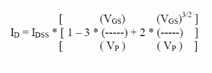
Id=Idss*(1-Vgs/Vp)^2
and transconductance is:
|d(Id)/d(Vgs)|=2*Idss*(Vt-Vgs)
This is how I would match JFETs (and, FWIW, MOSFETs as well) if I would have today an automatic test equipment. It can be done by hand, but it's very tedious and for 99.99% of applications pretty much not required:
For N channel: choose a very small Vds, e.g. +50mV and monitor the drain current while stepping Vgs from Vp (which is < 0) up to zero. In between -Vp and 0, in linear coordinates, the plot Id=f(Vgs) will always have a linear region. Not at to high currents, where Lambda (aka channel modulation) counts and not at to low currents, where the subthreshold conduction cannot be neglected. Identify this linear region and extrapolate the straight line on the graph, until it intersects the Vgs axis. The (negative) value is called "extrapolated threashold" Vpe and has the remarkable property of not depending on the JFET channel geometry variations.
Sort the devices in Vpe classes of your choice. Within each class, sort by Idss using the known method (Vgs=0, and e.g. Vds=5V) or match devices for Idss using your favorite null method.
You now got a population of devices that have both Vp and Idss matched (and hence also matched transconductance).
If you want to expand the matching over a large range of drain currents (which, btw, for JFETs should be always < Idss) you would have to include a third parameter that is Lambda. The equation is:
Ids-l=Ids*(1-Lambda*Vds)
Unfortunately, there's no longer a convenient way to extract the extrapolated threshold. You need to repeat the above procedure at at least two different (but still small) Vds and then use some sort of nonlinear regression to extract both Vpe and Lambda. Complicated and a pretty much useless exercise for any audio applications.
For P channel devices: mirror everything against the vertical (Ids) axis and take a negative small Vds.
AndrewT said:yes, I have.
I find little correlation, although others have posted the opposite view. Maybe we test differently.
I think Vbe and Vgs are far more important, then I select for a close match of gain (hFE) or transconductance (gfs). BUT ALWAYS at operational quiescent currents.
I am not usually able to test at operational Vce nor Vds, due to dissipation limitations, but I doubt our disagreement is due to this lack of ability.
As an aside I used to measure hFE first and then try to select similar Vbe from the close batches. It was a complete waste of my time.
The Vbe matches could come from any hFE batch.
I now test Vbe first. Batch them according to this parameter.
The slight problem with this is that the next amplifier may run at a different current and that initial selection must be rechecked at the new current.
Reading about the arguments for vbe or hfe matching I decided to do a quick test if their was any corrolation between them as you found there not to be. I usually matched for hfe in my projects although I rarely do so because of buying matched pairs. My reciept only states matched hfe and I have no idea how it was done.
I used 2 different Sanyo transistors, 2sc2911 and 2sc2362k. I cannot be 100 percent conclusive because these parts ,2sc2362, were matched by factory but either they went through a lot of trouble or there is a corrolation.
With 2sc2362 pairs that were supplied as matched pairs with hfe +- 5 percent or better matched I find the vbe s to be closely matched too, sometimes even closer matched. All the parts are from the same batch and I cant see parts from different batches used to get first vbe s matched then hfe s.
With the 2sc2911 I find the same corrolation. These were matched to their complementary but taking a few npn s from same batch and matching their hfe s to within 5 percent I find their vbes to be closely matched too.
This is just the opposite from what you said above

Can anyone else try this, maybe with parts from a different manufacturer.
syn08 said:
Id=Idss*(1-Vgs/Vp)^2
Oversimplified textbook true. No real part behaves like this.
Janneman
---This Perrot is that the guy aka Hephaistos?---
Hephaistos was Gérard Perrot's pseudo for the articles he published in french magazine "L'Audiophile". A great part of them were about the design of very linear transistorised circuits aimed to avoid thermal distorsion.
---This Perrot is that the guy aka Hephaistos?---
Hephaistos was Gérard Perrot's pseudo for the articles he published in french magazine "L'Audiophile". A great part of them were about the design of very linear transistorised circuits aimed to avoid thermal distorsion.
I think Schockley 1952 yields the same equations. The excellent Japanese work in the 70's unfortunately uses the atan function for fitting.
This matching stuff can be "make work" If I have a circuit with two FET's and four resistors and force the resistor values and pick FETs for a perfect output or do the visa-versa, what's the difference? Maybe there's a difference large signal maybe not, build and see.
This matching stuff can be "make work" If I have a circuit with two FET's and four resistors and force the resistor values and pick FETs for a perfect output or do the visa-versa, what's the difference? Maybe there's a difference large signal maybe not, build and see.
PMA said:
Oversimplified textbook true. No real part behaves like this.
PMA said:This is much better. + channel length modulation, that depends on Vds.
Excellent, you must be my electron device physics PhD advisor in disguise

Seriously, before copy/pasting and declaring "much better" such, you'd better do your homework and make sure you understand when, where, for what devices and under which circumstances this formula holds.
Anyway, it does not include any channel modulation effect due to the longitudinal field (which is what counts an any device since the 60's) and is simply the result of a series expansion of the atan model that Scott mentioned. For all practical purposes, it isn't in any way shape or form much better than the classic parabolic and Lambda corrected Id=f(Vgs) for any devices currently available.
Here's a comparison between the two approaches.
And BTW, your beloved Spice you used to prove to the world the JFET matching benefits uses exactly the parabolic model with Lambda channel modulation
forr said:Janneman
---This Perrot is that the guy aka Hephaistos?---
Hephaistos was Gérard Perrot's pseudo for the articles he published in french magazine "L'Audiophile". A great part of them were about the design of very linear transistorised circuits aimed to avoid thermal distorsion.
OT
That's what I thought. I have a lot of "Audiophile" articles by him (and Jean Hiraga), great articles, that mostly didn't get the exposure they earned, possibly because they were in French. But they were at least as good and astute as anything in the English press at the time.
/OT
jd
john curl said:And people wonder why I just measure, rather than model!
With you there, John.
Nelson Pass said:
With you there, John.
I even solder sometimes a real application before measuring.
Hi Jan,
In fact, I had begun a practice of measuring distortion before and after the matching process. The measured performance was not that different, but then I was measuring total harmonic distortion only. The reason for this was that I had always matched transistors in the long tailed pair. I was taught that the hFE was the critical parameter, and it made sense to me that it would. After all, the diff pair's job is to compare the input signal and output signal, then to correct to reduce the error term (the difference). Complex math was never required for this. The concept is dead easy to understand.
Anyway, for a number of years, customers would come back, or call, asking what I had done to make the amplifier sound better. I was baffled for a long, long time. After all, I was merely following the directions in the service manuals and application notes that I still read today (current material, although I do refer back from time to time). I didn't occur to me that the beta matching of input pairs was as critical as it seems to be. That's why I started to examine what the effects of what I was doing were.
This never seemed to be questionable in any way. It wasn't until I began reading posts here that there was cause to re-examine what I had accepted for so many years. I must say that from the continuing tests I had been doing, the "match by beta" idea has only been re-enforced over the years. Another thing I've noticed is that vBE is a parameter that varies as temperature and process more than anything else. It seems to be that beta is the variable that needs to be nailed down.
Sorry, a very long winded way to say that the information Mr. Self has published does agree very well with what I have observed for so long.
The concept of negative feedback hinges on something we take for granted. We are assuming that the summing point is balanced and works as advertised. Well, if those two transistors are not matched, the differential pair does not properly extract the difference information. It will then introduce more distortion and fail to fully correct the existing error. As the mismatch becomes greater, the problems grow greater, but at an accelerated rate. This agrees with a chart I saw in his third edition book on page 81, figure 4.6. I am sure glad I bought his (excellent) book, it gave me something to refer to since I am unpublished. Actually, the first few lines at the beginning of chapter 4 illustrate this point very clearly. The first author in a long time that I've agreed with so strongly.
Now, my understanding may be at fault here. Please, feel free to comment.
-Chris
Yes. He outlined that both in his book and from some other material he had prepared (or had prepared). I found this to be comforting since I had been seeing this in a practical sense for many years. Do, then measure.One point he made was that if you use a servo to correct DC offset from a non-matched diff pair, you also base the pair off of the center point where the transfer function is as linear as it gets. Any off-centering (which the servo would do) would place the pair in a less linear region.
In fact, I had begun a practice of measuring distortion before and after the matching process. The measured performance was not that different, but then I was measuring total harmonic distortion only. The reason for this was that I had always matched transistors in the long tailed pair. I was taught that the hFE was the critical parameter, and it made sense to me that it would. After all, the diff pair's job is to compare the input signal and output signal, then to correct to reduce the error term (the difference). Complex math was never required for this. The concept is dead easy to understand.
Anyway, for a number of years, customers would come back, or call, asking what I had done to make the amplifier sound better. I was baffled for a long, long time. After all, I was merely following the directions in the service manuals and application notes that I still read today (current material, although I do refer back from time to time). I didn't occur to me that the beta matching of input pairs was as critical as it seems to be. That's why I started to examine what the effects of what I was doing were.
This never seemed to be questionable in any way. It wasn't until I began reading posts here that there was cause to re-examine what I had accepted for so many years. I must say that from the continuing tests I had been doing, the "match by beta" idea has only been re-enforced over the years. Another thing I've noticed is that vBE is a parameter that varies as temperature and process more than anything else. It seems to be that beta is the variable that needs to be nailed down.
Sorry, a very long winded way to say that the information Mr. Self has published does agree very well with what I have observed for so long.
Actually, this is exactly the match is so critical. How does using nfb reduce the distortion produced in the diff pair if they are not matched? This is really an important point from what I understand.Intuitively I feel that the effect should not be very great, and there is still the global nfb to straighten things out, but the effect is there and can be measured on the ol function.
The concept of negative feedback hinges on something we take for granted. We are assuming that the summing point is balanced and works as advertised. Well, if those two transistors are not matched, the differential pair does not properly extract the difference information. It will then introduce more distortion and fail to fully correct the existing error. As the mismatch becomes greater, the problems grow greater, but at an accelerated rate. This agrees with a chart I saw in his third edition book on page 81, figure 4.6. I am sure glad I bought his (excellent) book, it gave me something to refer to since I am unpublished.
Actually, the first few lines at the beginning of chapter 4 illustrate this point very clearly. The first author in a long time that I've agreed with so strongly.Now, my understanding may be at fault here. Please, feel free to comment.
-Chris
Hi Joshua,
When matching any transistor types, temperature will be the biggest challenge. Everything shifts as the temperature changes. That is why I match power devices by roughly controlling the temperature. For all signal devices, I match them in a jig I built that is a differential pair, with no feedback. I select the tail current and vDS and allow the pair to settle in. They are in physical contact and surrounded by a foam cover. I have mentioned this before, and I have posted the circuit a couple times as well. Basically, the parts are experiencing very similar conditions that they would see in actual use. The degree of matching is indicated by the voltage on their collectors (drains) across a pair of tightly matched resistors. The base (gate) resistors are also tightly matched. This setup is valid for pairs that are matched, not when the collector (drain) voltages differ. Since it is a match we want, no problem. As I have implied, the matching jig is both sensitive and works well for both BJT and FET type transistors.
-Chris
Well, Pavel was quick and (correct) to answer that. Like many others, I don't have the ability to run curves on my components, so I spot check a few things. The pinch-off voltage and Idss are the two parameters I look at. If the job is really critical, then maybe a couple more points are measured. That's really a cross-check on my previous work. The transfer characteristic will line up pretty close as long as you can define two widely spaced points on the curves. Thank goodness for that!What would you match for JFETs in complimentary differential pairs, other than IDSS?
When matching any transistor types, temperature will be the biggest challenge. Everything shifts as the temperature changes. That is why I match power devices by roughly controlling the temperature. For all signal devices, I match them in a jig I built that is a differential pair, with no feedback. I select the tail current and vDS and allow the pair to settle in. They are in physical contact and surrounded by a foam cover. I have mentioned this before, and I have posted the circuit a couple times as well. Basically, the parts are experiencing very similar conditions that they would see in actual use. The degree of matching is indicated by the voltage on their collectors (drains) across a pair of tightly matched resistors. The base (gate) resistors are also tightly matched. This setup is valid for pairs that are matched, not when the collector (drain) voltages differ. Since it is a match we want, no problem. As I have implied, the matching jig is both sensitive and works well for both BJT and FET type transistors.
-Chris
Hi Bonsai,
I guess the big test for you would be to attempt a closer match and see if anything gets better. If there was anything that might mask the effect, you may not be able to tell. After all, your reference is usually the best thing you have heard so far.
One more comment, partly a joke. There are plenty of audiophiles around that think a Shure V15 MKIII sounds smooth. 'nough said right there.
Hi Andrew,
-Chris
It's possible that your match is good enough, I can't say because this is your work.I am using 4 bipolar input devices on my amp and my source and speakers are quite good - I don't pick up the brittle sound you mention. Betas were matched on a meter to within 10%.
I guess the big test for you would be to attempt a closer match and see if anything gets better. If there was anything that might mask the effect, you may not be able to tell. After all, your reference is usually the best thing you have heard so far.
One more comment, partly a joke. There are plenty of audiophiles around that think a Shure V15 MKIII sounds smooth. 'nough said right there.
Hi Andrew,
That's possible. But you did mention you didn't have access to a THD meter? An HP 3586A, 3581A or 3580A would have worked well for you. To be honest with you, a lack of more advanced equipment can blind you to things simply because you are unable to measure them. This may explain why you don't see the things I am. The beta test on DVMs are not reliable, and the temperature will be your greatest 2nd variable that you can not really control. If the temperature can not be controlled, you must then test in a way that cancels temperature changes. You need to test them in pairs that share a common thermal environment.Maybe we test differently.
-Chris
Hi Andrew,
Hi Jan,
-Chris
Don't feel bad. I can't either. Since we can't change this, reduce your measurements sensitivity to temperature.I accept that I cannot hold a device to a set temperature.
Here is where we differ. Only my emitters (sources) are connected directly together. I like to be able to measure base current in some way.I set up a long tail pair with the bases/gates directly connected.
I also directly connect the emitters/sources.
Yes.Now add a pair of accurately matched collector/drain resistors.
I use a current sink for the pair. The base will automatically draw the current it needs. vBE differences will certainly affect the outcome at this point in the test. The parts are tested in the sme manner that they are used in.Apply a Vbe/Vgs and measure the difference in collector current.
Of course it will. They way I do it, each transistor is free to settle in where they "want" to be. That means they are also free to shift the balance of tail current. You have forced a situation where the bases (gates) are forced to the identical voltage and emitter (source) voltage.This measurement method with Zero value for the External emitter/source resistor gives a very different result compared to Anatech's method.
Yes, that is correct. That is also why the emitter (source) connection is common to both devices.The zero Re is very intolerant of Vbe differences.
Hi Jan,
Exactly! Thats why many designs really don't need a servo. The DC offset can be brought less than 10 mV in practice without any heroics. I guess someone out there decided that DC offset must be less than 2 mV.One point he made was that if you use a servo to correct DC offset from a non-matched diff pair, you also base the pair off of the center point where the transfer function is as linear as it gets
-Chris
- Status
- Not open for further replies.
- Home
- Member Areas
- The Lounge
- John Curl's Blowtorch preamplifier part II