My "Lil Tiger" became a sub amp with the addition of an active filter and accompanied my Sinclair for many years. That was ~1975 before subs were common so people were impressed. Both blew up more than once and had the outputs replaced with bigger transistors. TO-126 transistors are not really big enough for even 10 Watts. Eventually, I removed the Sinclair modules and built a better amp from scratch, but I learned a lot form Sinclair. They moved with me to Edmonton, and they are somewhere in my junk in the basement here in the US. Later I bought a Pioneer receiver, but it never sounded as good as my home-made stuff. I have a couple old receivers that people gave me because they were dead. I spent a lot of time breadboarding circuits like the JLH but I was never very happy with them. Today, it's 2.1 channel computer speakers and Bluetooth, and LT Spice instead of breadboarding. Maybe I'll actually build something again now that I'm retired but I'm busy enough with the honey-do and dad-do lists.
Things are looking up. A little past 16V output. My god Mooly, you fixed it! Thank you very much.
") well that's good. At least the amp is 100% short circuit proof.
well that's good. At least the amp is 100% short circuit proof.I simulated a concept amplifier based on the JLH Class A three years ago. This uses a constant current load for the split load driver transistor - serving the Vas in a similar way to a Class B design. This excludes the resistor between Q1 collector and the positive power supply. R5, is used to provide emitter feedback to Q1 instead.
The set up of the constant current load was to allow variations in current by selecting suitable values of R2 to suit variations in output power level needs.
As there are no driver transistors for each power output device , the split load driver transistor has to deliver more current to energize two devices rather than one while operating in Class A. The aspirations should be sensible as suitable transistors would need to the used for a split load driver.
The supply rail voltages +/- 18 volts would to allow IC op.amps to be used as line stages. I envisaged a closed loop gain of 2 for such. It was convenient these supply voltages would meet that need while also allowing 15W peak outputs into 8R
The standing current of the output stage is adjusted by R6 between Q1 base and the amplifier output terminal this to divert a measure Q1 base current in this case 6 m.a. and reducing Q1 base current. Increasing R6 in value or removing it entirely increases standing current.
An additional feature when connecting between the output terminal R6 is that this establishes a short internal loop for negative feedback from the output terminal to reach the base of Q1.
The effect of this signal on Q1 base and that generated at the collector of Q3, will be summed finally by the global feedback network involving R1 and associated network components.
Q5 should be situated on the heat sinks to monitor thermal conditions and prevent overheating.
R10 is to buffer the output against reactive loads. JLH used this strategy in later designs this approach also can be seen in most Naim power amplifiers.
The front end of the design has a long tail pair of transistors which makes the complete circuit a radical departure from the original script. I have not built this as I have not found the time to do so due to personal circumstances.
The full circuit has stability margins for gain - circa 44 dB and phase margin - circa 90 degrees and is stable at unity gain
The THD levels are below those of the original design. It will tolerate parallel capacitor loads up to 470nF//8R at 15.5V peak outputs at 20kHz with THD <0.1%
At 4V peak outputs it will tolerate 2uF//8R at 20kHz with THD <0.05%.
I have simulated square wave tests with 8R//470nF to 15V peak which is a reasonable test limit.
Attachments
My "Lil Tiger" became a sub amp with the addition of an active filter and accompanied my Sinclair for many years. That was ~1975 before subs were common so people were impressed. Both blew up more than once and had the outputs replaced with bigger transistors. TO-126 transistors are not really big enough for even 10 Watts. Eventually, I removed the Sinclair modules and built a better amp from scratch, but I learned a lot form Sinclair. They moved with me to Edmonton, and they are somewhere in my junk in the basement here in the US. Later I bought a Pioneer receiver, but it never sounded as good as my home-made stuff. I have a couple old receivers that people gave me because they were dead. I spent a lot of time breadboarding circuits like the JLH but I was never very happy with them. Today, it's 2.1 channel computer speakers and Bluetooth, and LT Spice instead of breadboarding. Maybe I'll actually build something again now that I'm retired but I'm busy enough with the honey-do and dad-do lists.
I have not heard of "Lil Tiger" is this a derivative of a 1970s era South West Technical Products 250W design by Daniel Meyer? This design was examined by a contemporary designer whose name I do not recall. Whoever that may have been, at the end of his summary he wrote" Where are you Daniel Meyer?"
A passing acquaintance owned an Ampzilla from the same era which at the time I listened to. I thought it was ahead of its time since it was full complementary symmetry circuitry throughout. I don't have the SWTP Tigersaurus circuit with a similar concept except the output stage was quasi complementary.
Scans of old Popular Electronics magazines are on-line at https://frankosite2020.com/SWTPC-ARK/index.html and probably others. Looking at these today, they seem crude, even foolish with no emitter resistors in the Lil Tiger, and tiny TO-126 output transistors. At the time, that was all I could afford the larger Tiger amps were completely out of reach to me. At that time "solid-state" amps were notoriously unreliable and Tiger amps were no exception. I spend hours "designing" elaborate amp circuits that were nearly impossible to stabilize because I did not well understand feedback. I think my Lil-tiger ended up with TIP33, TIP34 outputs mounted on a chassis heatsink. That was a very long time ago. Then and now, there are a lot of enthusiastic "designers" who make things that soon fail because they do not know or care about reliability. People with too much money put up with this believing it goes along with "high performance".
My first Hifi was a Sony HP150 with about 8Watts rms output. The amplifier was housed under a low cost record deck. It had no cueing lever. I built the 1969 JLH and had it checked out a School Hobby night class in 1976. 20 years later I built the JLH1996 and gave the old hardware away. I'm still using the 1996 the system is quite bulky and the regulated power supply still has 33000uF of capacitance in each rail and this including a large toroidal transformer is housed in a separate box with an umbilical cord connection the the power amp and a second box for the pre-amp. I listen to this in our garage as my wife who is blind doesn't like the sort of music I prefer some pop and quite a lot of classical. As built I did not include the constant current NPN transistor on the main heat sink instead
I lowered the output current a smidgen while I could alter that the outputs are Onsemi 2N3055 which can handle the heat sink temperature max - in summer 60 degrees C. I can open the garage car entry door and some windows as we live on a hill and where it is a bit more airy than on the flat.
I lowered the output current a smidgen while I could alter that the outputs are Onsemi 2N3055 which can handle the heat sink temperature max - in summer 60 degrees C. I can open the garage car entry door and some windows as we live on a hill and where it is a bit more airy than on the flat.
Your angel wife has suggested you need a hobby. She would be doing that in your best interests - in your place I would be making her happy. In a recent post you showed some interest in working with LT Spice. I hope you take on the challenge, when I did that in addition to technical matters I also learned something about myself.
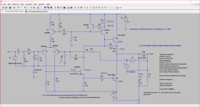
This is the output stage referred to. I tried to send this an .asc attachment however it is a long time since posted such an attachment and these are not accepted in the new site.
Zip files are allowed but if the content is .asc the file does not take. The value for C4 is extreme- that is at 15 W on 10kHz square wave output into 8R//470nF.
Q8 should be sited on the heat sink close to the output transistors. This and Q5 form a standard constant current structure, where Q8 heats up and draws more current through R11 which connects to ground at one end. Since V=IR there has to be an upward movement of Q5 base toward the voltage rail. Q5 vbe is less and so is Q6 base current.
Somewhere in his writing JLH suggested Q7 could be a MJ3001 a Darlington type in a TO-3 package. There was no suggestion of using this in place of Q6. 10kHz square wave 8R//470nF is shown. C4 has been increased for this test the standing current is not sufficient to do any better. The heat dissipation should be over 50% less than the JLH1996 that I built. The hardware is bulky and the power supply and preamp are in separate boxes from the power amp.
THD at 1W 20kHz 8R//470nF 0.006%
Attachments
Zip files are allowed but if the content is .asc the file does not take.

Test:
Edit... both attach as normal. .asc has always been a recognised file type since we moved to the new platform.
Attachments
Since others have posted full circuits for variations on the JLH Class A theme I see no barrier now to sticking my neck out on that count.
I will post the .asc files in due course.
The type of LTP circuit follows an unusual theme from a Naim amplifier thread from way back in time.
Why I have adopted this is explained as follows.
The collector currents through Q1 and Q2 are still a good match. Apart from d.c. current, a.c. current will flow through diffusion capacitance between the transistor's collector to base junctions. This diffusion capacitance is inversely proportionate to the square root of the voltage applied at the collector.
The voltage drop across load resistors 1k (Q1) and 4k7 (Q2) for equal currents will be greater for Q2 which will develop the greater level of collector to base capacitance. Such is indicative of the width of a transistor base region which in this instance will become greater in relation to the width of the collector.
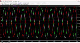
The effect of this is shown in the green plot in the second attachment as a loss of current gain. In semiconductor parlance this is known as base-width modulation
The collector to base capacitance of Q2 provides a measure of low pass filtering for the negative feedback signal. In an earlier simulation Q7 was a 2N3904 transistor suitable for 18 Volt supplies. The stability margins with this device are much improved over 2N3019 an after thought for increased supply rail voltages.
I will post the .asc files in due course.
The type of LTP circuit follows an unusual theme from a Naim amplifier thread from way back in time.
Why I have adopted this is explained as follows.
The collector currents through Q1 and Q2 are still a good match. Apart from d.c. current, a.c. current will flow through diffusion capacitance between the transistor's collector to base junctions. This diffusion capacitance is inversely proportionate to the square root of the voltage applied at the collector.
The voltage drop across load resistors 1k (Q1) and 4k7 (Q2) for equal currents will be greater for Q2 which will develop the greater level of collector to base capacitance. Such is indicative of the width of a transistor base region which in this instance will become greater in relation to the width of the collector.
The effect of this is shown in the green plot in the second attachment as a loss of current gain. In semiconductor parlance this is known as base-width modulation
The collector to base capacitance of Q2 provides a measure of low pass filtering for the negative feedback signal. In an earlier simulation Q7 was a 2N3904 transistor suitable for 18 Volt supplies. The stability margins with this device are much improved over 2N3019 an after thought for increased supply rail voltages.
Attachments
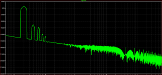
Tianplot simulation attached for Circuit detail in post 9454 above. Worked example also attached. R2 can be changed to alter the collector to base capacitance in Q2. Reducing R2 will reduce the latter capacitance. Check this in consideration of other tests such as 10kHz square wave with a capacitor in parallel with a resistive load - these are yet to follow.

Attachments
I'm not sure it matters much but, in post #9454 the schematic shows the Tian current source in parallel with the voltage source, which is incorrect. The current source should return to ground.
I agree that the JLH amp is unnecessarily crude, and extensions are well worth the pennies for an LTP etc. Initially, I was just a bit disgusted, but I found that there is merit to the idea if you clean it up with, for example, equal loading on both sides of the VAS/ driver and an offset to the upper OP. The attached MOSFET version provides respectable THD performance and rail-rail output, and operates class-AB.
I agree that the JLH amp is unnecessarily crude, and extensions are well worth the pennies for an LTP etc. Initially, I was just a bit disgusted, but I found that there is merit to the idea if you clean it up with, for example, equal loading on both sides of the VAS/ driver and an offset to the upper OP. The attached MOSFET version provides respectable THD performance and rail-rail output, and operates class-AB.
Attachments
I'm not sure it matters much but, in post #9454 the schematic shows the Tian current source in parallel with the voltage source, which is incorrect. The current source should return to ground.
Correct in both cases. The error is due to a one off move too far with the drag tool. It is simple enough for those interested to amend the simulation. Sorry about that.
The attachment here contains a series of tests.
Where the script is in blue this is comment - as distinct from a SPICE directive. This should be obvious from the dialogue.
One can click on either to bring up options to change status.
This circuit lacks the ability to increase current as a Class AB amplifier can do. For the parallel limit for square wave during t.on of 50us is 470nF. Individual transients do not last that long. To be continued.

- Home
- Amplifiers
- Solid State
- JLH 10 Watt class A amplifier