Hello Gabor,
Here are the diy files and gerbers. All the best for your build") .
.
if there is GB to be organized, i could do that, let me know. I have asked manufacturer for a quote.
reg
Prasi
Here are the diy files and gerbers. All the best for your build
. if there is GB to be organized, i could do that, let me know. I have asked manufacturer for a quote.
reg
Prasi
Attachments

Last edited:
Well I was wondering abt mtg arrangements for the TO-3, Gabor said he will use flat aluminium angle to mount PCB.
But as per http://www.ti.com/lit/an/sboa020/sboa020.pdf ,
the direct PCB mount method is only suitable for low dissipation.
The arrangement given in fig 4 right bottom is still PCB mount method but with a spacer (2-3 metal washers?).
I want to know whats preferred by builders. run wires? or aluminium angle method+spacer?
It will then help me to decide preferred hole dia (for B and E) and pad sizes (C1 and C) for the MJ15003.
Hello Gabor,
Here are the diy files and gerbers. All the best for your build
if there is GB to be organized, i could do that, let me know. I have asked manufacturer for a quote.
reg
Prasi
You are the best [emoji120]
Tapatalk kullanarak iPhone aracılığıyla gönderildi
Well I was wondering abt mtg arrangements for the TO-3, Gabor said he will use flat aluminium angle to mount PCB.
But as per http://www.ti.com/lit/an/sboa020/sboa020.pdf ,
the direct PCB mount method is only suitable for low dissipation.
The arrangement given in fig 4 right bottom is still PCB mount method but with a spacer (2-3 metal washers?).
I want to know whats preferred by builders. run wires? or aluminium angle method+spacer?
It will then help me to decide preferred hole dia (for B and E) and pad sizes (C1 and C) for the MJ15003.[/QUO
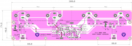
Hi Prasi
Thank you for the nice layout, excellent work!
If one use wires to mount the power transistors the whole PC board design was vain.
For $10 a pair I (we)could get a pair from Ebay and use wires to connect the power transistors. I only can use the TO-3 transistors if I use L or T shape aluminium to mount it to my heatsink. The center of the heatsink where I can mount the transistors are 22mm thick. Other option would be the TO-3P or TO-264 plastic case. I am not sure that can handle the heat. To use 3 pair is a other option but we run int several issues. If we ad a extra pair power transistor may be we need to mode the circuit, and the PC bord become useless. (almost)
I built a Hiraga 30W with one pair (24V rail voltage) TO-3 power transistors and had no problem at all using L shaped profile. Sorry I just woke up and I can not think straight. I hope the PC board design not just for me, I see some interest but do we have enough people for a small GB that a question to.
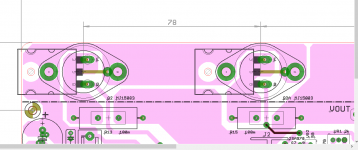
Prasi, no worries- you have a universal pcb design that can accommodate both MJL4281 TO264 ot MJL15993 To3 cases. If flatpack are used the you will mount under the board and the whole PCB flat to the heat sink This arrangement will allow more free space for power conditioning..
When using the TO3 packages the L bracket could be used. These two transistors foot prints actually overlap wonderfully.
I am giving you good mechanical ideas.
When using the TO3 packages the L bracket could be used. These two transistors foot prints actually overlap wonderfully.
I am giving you good mechanical ideas.
Hi Nico,Prasi, no worries- you have a universal pcb design that can accommodate both MJL4281 TO264 ot MJL15993 To3 cases. If flatpack are used the you will mount under the board and the whole PCB flat to the heat sink This arrangement will allow more free space for power conditioning..
When using the TO3 packages the L bracket could be used. These two transistors foot prints actually overlap wonderfully.
I am giving you good mechanical ideas.
You have been extremely helpful. Your post gave me the below idea.
This is what could be done to fit either TO-3 or TO-264.
Regards
Prasi
Attachments
Last edited:
Hi Nico,
You have been extremely helpful. Your post gave me the below idea.
This is what could be done to fit either TO-3 or TO-264.
Regards
Prasi
Excellent, just make a note to mount the TO263 under the board. Truly universal!

I run into some problem with these project I can not resolve it.
If you look at my heatsink I only can mount the transistors or the L shape profile on the smooth surface area (marked by red)
The place marked by yellow is taller by 1 or 2MM. To have firm contact and good heat transfer each side I have to use 2 PC L profile for the TO-3 transistors
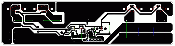
For that reason I modified the Prasi's layout..
Now I run into another problem.
All the tone-transfer papers come in A4 size or smaller so they are shorter than the actual PC board layout
I need the so called legal size paper to print it out (14 inch long).
Did someone ever used tone transfer (heat transfer) or any photo paper in that size? I made a couple doses of PC boards but never had these problem.
It look like I wasted my time to modify Prasi's layout and I am back to square one with these project.
I have to use fly wires to connect the power transistors (what I wanted to avoid at any cost)
Any advise welcome.. Thanks
If you look at my heatsink I only can mount the transistors or the L shape profile on the smooth surface area (marked by red)
The place marked by yellow is taller by 1 or 2MM. To have firm contact and good heat transfer each side I have to use 2 PC L profile for the TO-3 transistors
For that reason I modified the Prasi's layout..
Now I run into another problem.
All the tone-transfer papers come in A4 size or smaller so they are shorter than the actual PC board layout
I need the so called legal size paper to print it out (14 inch long).
Did someone ever used tone transfer (heat transfer) or any photo paper in that size? I made a couple doses of PC boards but never had these problem.
It look like I wasted my time to modify Prasi's layout and I am back to square one with these project.
I have to use fly wires to connect the power transistors (what I wanted to avoid at any cost)
Any advise welcome.. Thanks
Attachments
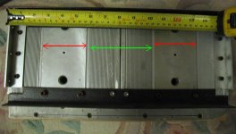
I run into some problem with these project I can not resolve it.
If you look at my heatsink I only can mount the transistors or the L shape profile on the smooth surface area (marked by red)
The place marked by yellow is taller by 1 or 2MM. To have firm contact and good heat transfer each side I have to use 2 PC L profile for the TO-3 transistors
For that reason I modified the Prasi's layout..
Now I run into another problem.
All the tone-transfer papers come in A4 size or smaller so they are shorter than the actual PC board layout
I need the so called legal size paper to print it out (14 inch long).
Did someone ever used tone transfer (heat transfer) or any photo paper in that size? I made a couple doses of PC boards but never had these problem.
It look like I wasted my time to modify Prasi's layout and I am back to square one with these project.
I have to use fly wires to connect the power transistors (what I wanted to avoid at any cost)
Any advise welcome.. Thanks
Hi Gabor,
the possibility that i can think are as follows
1. is possible to clamp the heatsinks and machine them (milling) in one go?
1a. alternatively, you could remove material in the yellow contact region from the L-bracket and have good flat contact at the red region. this will decrease the contact area between the bracket and heatsink and may not be good for heat transfer.
2. looks like you are short of toner paper by 3mm. can you attach a strip (1 inch may be) to it and tape it (with paper tape) from the backside and then use for toner transfer? if there are any discontinuities in toner, you could fill it with marker pen
2a. you could forgo the copper on either side of the layout by 3-5mm and still have a working pcb
. regards
Prasi
Last edited:
It's a class A amplifier so there are no fast switching currents to limit with PCB defined field cancellation techniques and very little to worry about with the use of short leads. They are only really required for one pair of output devices anyway.
Go ahead and prove the design with with one pair on a conventional board with pads for the second pair either side. Then add small outrigger boards later, to connect the second pair if all-PCB construction is important to you.
Really, the question is what advantage is there to using a PCB for connecting these power transistors rather than wiring, on a doubtful principle that performance should be better, as you might expect with a well designed class AB layout for the output stage. Otherwise, it can only be about visual, architectural aesthetics. I understand this desire but it will be difficult, as you find so far.
+1It's a class A amplifier so there are no fast switching currents to limit with PCB defined field cancellation techniques and very little to worry about with the use of short leads. They are only really required for one pair of output devices anyway.
Go ahead and prove the design with with one pair on a conventional board with pads for the second pair either side. Then add small outrigger boards later, to connect the second pair if all-PCB construction is important to you.
Really, the question is what advantage is there to using a PCB for connecting these power transistors rather than wiring, on a doubtful principle that performance should be better, as you might expect with a well designed class AB layout for the output stage. Otherwise, it can only be about visual, architectural aesthetics. I understand this desire but it will be difficult, as you find so far.
There is a reason I try to avoid to use wires to connect the power devices.
I tested with two different Class A amplifier, at AlephX for better heat spread and it took me almost a day to dis-ensemble and re-ensemble the whole case (about 20Kg heat sink) of the amp ad repeat it again.
Second amplifier the Hiraga Class A, I used pure silver wire in teflon tubing and silver plated Teflon wire (which was used previously as a speakers hookup wire from Peter Daniel) It was not the classic thin sounding cheap silver plated wire.
I still did not like to use it between the PC boards and the power devices. May be the silvered wire has that effect I don't know.
Yes I did A-B listening test.
I know many old school amplifier was built that way and few of them today to.
May be they knew something I don't.
I do not want to religiously argue over these, if I can avoid it to me the best way.
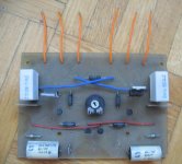
These was my Hiraga Class A 30W with TO-3 power device.
I tested with two different Class A amplifier, at AlephX for better heat spread and it took me almost a day to dis-ensemble and re-ensemble the whole case (about 20Kg heat sink) of the amp ad repeat it again.
Second amplifier the Hiraga Class A, I used pure silver wire in teflon tubing and silver plated Teflon wire (which was used previously as a speakers hookup wire from Peter Daniel) It was not the classic thin sounding cheap silver plated wire.
I still did not like to use it between the PC boards and the power devices. May be the silvered wire has that effect I don't know.
Yes I did A-B listening test.
I know many old school amplifier was built that way and few of them today to.
May be they knew something I don't.
I do not want to religiously argue over these, if I can avoid it to me the best way.
These was my Hiraga Class A 30W with TO-3 power device.
Attachments
- Home
- Amplifiers
- Solid State
- JLH 10 Watt class A amplifier