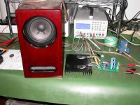
Today I'm sooooo happy with the testing result. After the following modifications of the original first design I posted:
1. VR1 changed to 100R
2. R13 changed to 10R
3. Q3 changed to BD139
The amplifier is working great! At the beginning the THD is 1% @1KHz/1W/8Ohm, pretty high for a class-A. I realize that Q1 and Q2 should be paired matched. Then I changed them with 2 pair matched transistors, the THD drops to 0.05%!
I also tried with some other transistors such as 2N3055, 2N3773 and finally 2SC5200. In my own opinion I like the sound of 2SC3280 most, high freq is very clear.
BD139 and BD140 works great in the testing. I think it's no need to worry about the high current. The don't have a heatsink and were slightly warm during working.
Hope your guys can also build a great amplifier when you receive my free PCBs.
Attachments
Last edited:
A transistor doesn't have to run hot to exceed SOAR.
Half waves of 20Hz are quite long for "pulse" operation.
An overstressed transistor will degrade over time due
to local spot heating, you can't detect from outside.
Granted, it might take 2n3055 and 4 ohm load to really
overstress the BD140 at Q8, but you certainly aren't
giving yourself much of a margin...
Hi kenpeter,
Thanks for figure out this problem. it's real a problem when the board works at high voltage and low impendance. I think it's better to supply the board with +-20V or lower, and don't push the power to high.
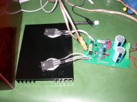
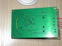
I also forget to say that one trace is missing for the first version. The collectors of Q3 and Q8 are not connected on the PCB. A fly wiring is needed here, see the photo below. It's connected in the version 2.
Thanks for figure out this problem. it's real a problem when the board works at high voltage and low impendance. I think it's better to supply the board with +-20V or lower, and don't push the power to high.
I also forget to say that one trace is missing for the first version.
The collectors of Q3 and Q8 are not connected on the PCB. A fly wiring is needed here, see the photo below. It's connected in the version 2.A transistor doesn't have to run hot to exceed SOAR.
Half waves of 20Hz are quite long for "pulse" operation.
An overstressed transistor will degrade over time due
to local spot heating, you can't detect from outside.
Granted, it might take 2n3055 and 4 ohm load to really
overstress the BD140 at Q8, but you certainly aren't
giving yourself much of a margin...
Attachments
2SC3421 doens't have a metal pad so it doesn't to assembly it on the same heatsink with BD140.
It's also OK to mount BD139 on the same heatsink with BD140 in this design (if using BD139 as replacement for 2SC3421). BD139 has a metal pad connected to collector. The 2 collectors are connected in this design.
It's also OK to mount BD139 on the same heatsink with BD140 in this design (if using BD139 as replacement for 2SC3421). BD139 has a metal pad connected to collector. The 2 collectors are connected in this design.
Hi all, just a quick question, is it ok to mount Q3 2SC3421 on the same heatsink as the output transistors or would it be best to use a seperate small heatsink for it. Which would be the best solution to keep Iq and offset most stable.
thanks for your help
Alan
Hi Ken,
Kindly explain why the BD140 would operate outside of its SOA if the voltage across it is48V, in other words both the driver transistor and 2K2 resistor happens to be short circuit, while the current remains limited to 30mA.
0.03 x 48 = 1.44 watt and very much inside the SOA curves. The BD140 is rated at 3.6 watt and there should not be a problem at all.
Attachments
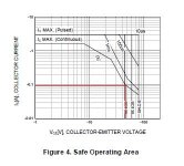
Then you do not allow anywhere enough bias for droopy old 2n3055!
This traditional JLH output transistor would not be much of an option.
Could require 144mA for an 8 ohm load, and 458mA for a 4 ohm load.
These figures based upon the LTSpice default model for 2n3055.
Ic(Dut2): 5.30091 device_current
Ib(Dut2): 0.457543 device_current
Ie(Dut2): -5.75846 device_current
Ic(Dut1): 2.77545 device_current
Ib(Dut1): 0.143543 device_current
Ie(Dut1): -2.919 device_current
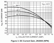
Based upon OnSemi spec sheet, we can see the typical beta droop.
24 volts into 4 ohm load is 6A, so something like 25 might be Beta....
6A / 25Beta = 240mA Base Current.
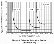
From same OnSemi spec sheet, we can look at collector saturation,
and see that 6A would drop about 0.8VCE, and that we can expect
a base current of around 300mA.
A volume of evidence here that 66mA might not be enough...
You could just let 2n3055 run out of steam at 66mA, and clip early.
But if you allow "enough" current for this transistor to go rail to rail,
BD140 would be at risk...
This traditional JLH output transistor would not be much of an option.
Could require 144mA for an 8 ohm load, and 458mA for a 4 ohm load.
These figures based upon the LTSpice default model for 2n3055.
Ic(Dut2): 5.30091 device_current
Ib(Dut2): 0.457543 device_current
Ie(Dut2): -5.75846 device_current
Ic(Dut1): 2.77545 device_current
Ib(Dut1): 0.143543 device_current
Ie(Dut1): -2.919 device_current
Based upon OnSemi spec sheet, we can see the typical beta droop.
24 volts into 4 ohm load is 6A, so something like 25 might be Beta....
6A / 25Beta = 240mA Base Current.
From same OnSemi spec sheet, we can look at collector saturation,
and see that 6A would drop about 0.8VCE, and that we can expect
a base current of around 300mA.
A volume of evidence here that 66mA might not be enough...
You could just let 2n3055 run out of steam at 66mA, and clip early.
But if you allow "enough" current for this transistor to go rail to rail,
BD140 would be at risk...
Attachments
Last edited:
You tried real 2n3055 with BD140 at 66ma, and it "worked"
just fine. I can easily believe that it sounded fine. But does
66mA allow this classic output perform as well as it should?
66mA base current into 2n3055 transconducts 1.75A peak.
Thats to say your JLH class A quiescent would be about 1A.
Quiescent always a little larger than 1/2 due to beta droop.
Nets only 12WRMS from a circuit that should do 30WRMS.
With a 4 ohm load, you can only get 6WRMS...
So it is no trivial flaw, this might want more base current
than BD140 can safely deliver! Its not hard to fix... Just
need a PNP with larger SOAR here at Q8, and wider range
of drive current adjustment, possibly to 500mA.
Last edited:
I'm just saying any 2n3055 should work. Not just the "special" ones...
Beta at 10mA has nothing to do with Beta once it begins to droop.
What was the point of matching at 10mA? Your outputs will spend
exactly how much time at 10mA? What was that quiescent again?
I've looked into the ST, but they do not show any curves.
Maybe some archive has an older version of the ST specsheet...
Note the emitter resistor in this test could cook 50W or more!
2W should do fine for the base resistor...
Attachments
Last edited:
Hi all, thanks for your reply Siliconray. My brain was not fully engaged when I asked if Q3 and Q8 could be mounted on the same heatsink as the output transistors, thinking about it it was a silly suggestion. However could I ask almost the same queston again- is it best to mount Q3 and Q8 on seperate heatsinks from one another or could they be mounted on the same heatsink (not the output heatsink)- which is the best solution for minimum Iq drift
thanks for your help
Alan
thanks for your help
Alan
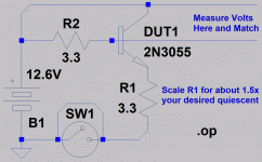
To do the matching properly, you need to match hfe at the working bias.
That means you need a special test rig to run the transistor at bias current and on heatsink.
In my balanced Xed JLH Class A (8x MJ21194 per channel), they were matched at 15V 1.4A, and I actually measured hfe from Ic of 0.25A to 2.5A dynamically using a triangular wave at the base pin at 100Hz.
http://www.diyaudio.com/forums/solid-state/3075-jlh-10-watt-class-amplifier-29.html#post942914
http://www.diyaudio.com/forums/solid-state/3075-jlh-10-watt-class-amplifier-31.html#post1108714
Patrick
Last edited:
we do seriously mathing in this way:
Matched:
Unmatched
Matched:
An externally hosted image should be here but it was not working when we last tested it.
Unmatched
An externally hosted image should be here but it was not working when we last tested it.
Hi Alan
The better way is the one that has less temperature increasing. Of course seperated heatsink will performance better if you have only a certain type of heatsink. But you can mount both on a larger heatsink to achieve better performance.
The better way is the one that has less temperature increasing. Of course seperated heatsink will performance better if you have only a certain type of heatsink. But you can mount both on a larger heatsink to achieve better performance.
Hi all, thanks for your reply Siliconray. My brain was not fully engaged when I asked if Q3 and Q8 could be mounted on the same heatsink as the output transistors, thinking about it it was a silly suggestion. However could I ask almost the same queston again- is it best to mount Q3 and Q8 on seperate heatsinks from one another or could they be mounted on the same heatsink (not the output heatsink)- which is the best solution for minimum Iq drift
thanks for your help
Alan
I do not think that I can agree with you Ken. At worst case the current gain of the 2N3055 according to the curves that you show is 50. With 3 Amps peak, the base current is only 60 mA. I would not expect an amp with 22V rails being earmarked for sound reinforcement.
Siliconray is probably considering a class A amp for domestic requirements using efficient, good quality 8 ohm speakers and not that of making a low voltage welding machine.
Siliconray is probably considering a class A amp for domestic requirements using efficient, good quality 8 ohm speakers and not that of making a low voltage welding machine.
Member
Joined 2009
Paid Member
Today I'm sooooo happy with the testing result
Nice work !
and those little red speakers look rather familiar... http://www.diyaudio.com/forums/full-range/175056-martello-enclosure-fr88ex.html#post2371641
> we do seriously matching in this way
If I can read correctly, you are measuring the transistors using a curve tracer at current levels of a few mA's. So you are assuming that the hfe of the transistor would be linear and constant from a few mA up to say 2A ? I presume you bias the transistors at Class A at say around 1A. Also are you assuming that the characteristics of the transistor would remain the same at room temperature and at say 60°C ?
> Of course seperated heatsink will performance better if you have only a certain type of heatsink.
I wonder if it is your experience that the output transistors have negative tempco and therefore there is no danger of thermal run-awy or the necessity of the lower transistor to thermally track the upper one for output DC stability ? Or you have a means of thermal tracking using separate heatsinks that you are willing to share with us ?
Regards,
Patrick
- Home
- Amplifiers
- Solid State
- JLH 10 Watt class A amplifier