I suspect that the engineering goals, with their emphasis on linearity, are not the same as the psychoacoustic ones, and moreover the latter are inconsistent as they depend on fatigue and other human factors.
Add to that the market biases we all have, you have a perfect marketplace for a diversity of products, all offering something slightly different, and some offering wonderful sound quality with lousy specs - like the single ended triode!
Why should audio be any different to other human endeavours, like breaking sporting records, eating, choosing a wife, dealing with conflict... not to be absurdly relativistic, but audio is for humans, not for cyborgs.
Cheers,
Hugh
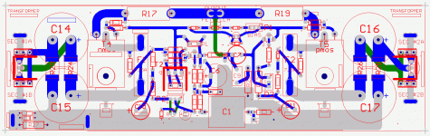
After conferring with Greg, I have attached the pcb design. It is two sided, 230mm x 69mm, for mounting directly above the outputs on a 250mm heatsink or longer. It will be gold immersion, 2mm FR4, with overlays on both sides; premium quality.
If anyone would like one of these boards, which will likely be priced around $USD50 for a pair (including shipping), would you please show your interest on the AKSA forum in a possible group buy? I will start a new sticky there for those who are interested.
The board is along the lines of a recent Aspen product and borrows from its power supply and output stage layout. Many hours have gone into this board. It is a proven layout, works very well, and should be easy to get going. I have left spaces for experimentation with lag compensation and phase lead. Jfets have large pads to help dissipate heat. Diodes used in the power supply are BYC28E-150, UFSR from Philips. Caps are 30mm diam, anything up to 6,800uF each side. Interelectrode resistors are 0R15 2W smds from Dale-Vishay.
The amp is configured for 36V rails, which require a 25-0-25Vac trafo rated to 225VA. This gives exactly 50W at peak, which is sufficient to drive almost any speaker. Remember, this is ONE channel only; the other is identical, but that does mean either two trafos or one with two connections for each secondary wire.
Cheers,
Hugh
Attachments
Last edited:
All,
Here it is, stable as the titanic on a lake.
Turned out it was the VAS gate stopper....thanks mikelm!
Miller cap not completely necessary but it does tidy it up a bit. Driving 100nF causes just the tinest bit of overshoot, not enough to concern me.
Sounds very good!
Here is an investigation, swordfishy
Is there any hint to the min-max value of gate stoppers
- for IRF9610
- for ZVP3310
Regards
Finally!After conferring with Greg, I have attached the pcb design. It is two sided, 230mm x 69mm, for mounting directly above the outputs on a 250mm heatsink or longer. It will be gold immersion, 2mm FR4, with overlays on both sides; premium quality.ondary wire.
-----
-----
Cheers,
Hugh
I think it is the first attempt to PCB.
I know you have experience from Aspen amplifiers.
THey have good PCB.
Great, Hugh!
I think this is close. But I do not know for certain.Hi all.
Hugh, very good.
What is the final scheme that corresponds to your PCB?
GEirin
In this post: http://www.diyaudio.com/forums/soli...as-lateral-output-perfect-23.html#post2609054
SWF later said that the schematic has an error. There needs to be a gate stopper on the DN2530. Let's be patient, no need to rush this. Let Hugh or SWF provide a final schematic.
Concerning the DN2530: Adding a gate stopper will decrease the CCS performance. To fix this I propose a small cap from G-S. I don't know how this will affect stability. I'll bet I'm too late though.")
- keantoken
Concerning the DN2530: Adding a gate stopper will decrease the CCS performance. To fix this I propose a small cap from G-S. I don't know how this will affect stability. I'll bet I'm too late though.
- keantoken
I rather doubt, Barmanekm, that the specs will be published on this amp as no one conveniently to hand has an AP2 Distortion Analyser. I can give you these simulated, preliminary specs, which hopefully we can confirm once a few have been built and measured:
THD is 0.010482% at 1KHz +20dBU (13W) into 8R
H2 is 77dB down for +20dBU output, 13W into 8R
96.8% of THD is H2, H3 and H4, all musical
Quiescent Current 370mA
However, if specs are your main aim, I think this amp is not for you. It does not measure that well by strict purist standards, though just how specs align with the sound quality remains a very good question, unanswered after sixty years. It is deep Class AB, however, and a very simple topology, all single ended except for the output stage, so the likelihood of it sounding good is a no brainer.
Post #1130 on page 113 shows the last schematic.
BTW, have a look at the layout, Kean, there is a gate stopper on the DN2530, and you might notice something else strange about it.....
I will leave posting of the final schematic to Greg. It's the AC coupled version, and uses 2SK170BL as input device and ZVP3310A as the voltage amplifier.
Hugh
Last edited:
Oh, do I spy positive feedback? To make the output stage "drive itself"? That's what I call initiative...
I can't remember whether I suggested that or not. I don't think so, but it was on my mind. Interestingly, I discovered in the simulator one day that if too much positive feedback was given back to the output stage, the input stage would just assume the opposite role of draining away the excess base drive from the output stage. I wonder if this works in real life? I imagine this would cause the harmonic phases to flip, I should experiment.
- keantoken
Hi all,
My apologies for being distant. I am on holiday for 3 weeks so I can't do too much, though I will be keeping an eye on the forums. Hugh's PCBs have an as yet unpublished circuit using a very special MOSFET bootstrap ccs. It offers all the pros and none of the cons of any ccs topology - very good regulation, latch up proof, very simple.
Hugh is also going with the irf9610 because that can be run at higher rail voltages for more power. I personally am happy with my 25v rails but both of us know some of you won't be.
I will post a schematic once I'm back unless Hugh beats me to it.
I found in the simulator a resistor was needed in series with the cap to keep the amp stable. My simulation was best with 808pF+510R. (using the IRF9610 VAS, k1058/j62 and DN2540 depletion FET since I didn't have a model for the DN2530)
I will wait eagerly for the final schematic.
- keantoken
I will wait eagerly for the final schematic.
- keantoken
Any progress there mikelm?
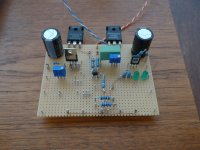
Switched on one board yesterday
low bias, no heat sink. Looked good & stable on the scope, should hear some sounds today and see some square waves a few days after - building a little sq wv gen kit till my signal generator arrives.I'll build four boards like this so I can play around with it and compare different versions easily.
When it's finalised, I'll do a PCB and order some premium components.
mike
Attachments
Last edited:
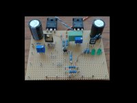
Superb photograph.Switched on one board yesterday
I'll build four boards like this so I can play around with it and compare different versions easily.
When it's finalised, I'll do a PCB and order some premium components.
mike
Why so big?
Here are two edited examples, one @ half file size and the other at one quarter of file size.
Is the extra detail shown in the original worth a file 4 times as large?
Attachments
Last edited:
- Status
- This old topic is closed. If you want to reopen this topic, contact a moderator using the "Report Post" button.
- Home
- Amplifiers
- Solid State
- JFET input, MOSFET VAS, LATERAL output = Perfect!!