The Vgs that are up around 700mV are quite high.
That indicates you are pulling a lot of current through them.
Try increasing the Rs of the lower device. Try going to 470r and if that is too high add in a parallel resistor until you get Vgs into a range you consider acceptable.
Then swap out the 470r+parallel to a fixed resistor.
Compared to the others I would aim for <400mVgs.
Did you select your devices by Idss (Vgs=0), or by Id for a fixed -Vgs?
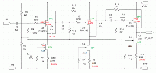
It adds a resistor into the vertical string from Follower to CCS.
Then you take an output tapping from below the added resistor.
Since your devices are different you may need to adjust the added resistor slightly to take account of tempco.
Using the same value as the lower Rs will get you very close to gate voltage and that in turn means all the Vgs add up to a very small offset in the LP filters.
You can do the same in the HP filters, but because they don't add up, they don't end up with an enormous offset.
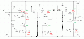
Last edited:
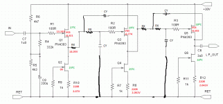
as before, you wired it up wrongly or overheated a device.Any idea how to fix the positive VGS of Q3 (HP board I)?
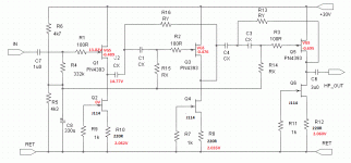

I think I have this back to front. Before you remove the 220r,The Vgs that are up around 700mV are quite high.
That indicates you are pulling a lot of current through them.
Try increasing the Rs of the lower device. Try going to 470r and if that is too high add in a parallel resistor until you get Vgs into a range you consider acceptable.
Then swap out the 470r+parallel to a fixed resistor.
Compared to the others I would aim for <400mVgs.
Did you select your devices by Idss (Vgs=0), or by Id for a fixed -Vgs?
try reducing Rs slightly by adding a 510r in parallel and measure the new Vgs of the upper device. If Vgs has increased then go the other way. If Vgs is decreased (from -700mVgs to -400mVgs) then you have moved in the right direction.
That puts all three Buffers at near the same Vgs.
This Buffer is passing a bit more current and will run hotter.
Calculate the new resistor (use either 130r or 150r) and then measure the new Vdrop. After that check the Vds of both the upper and lower devices and then calculate the Pq of both.
Are they OK or too hot for long term reliability?
Do any of the devices need a "flag" heatsink?
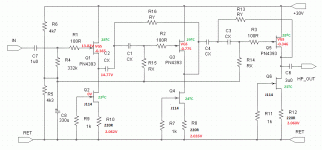
I don't believe your measurements.
You have 30V available shared between two transistors and a resistor.
The resistor passes ~10mA and drops ~2V.
That leaves 28V @ 10mA to be dissipated in the two transistors.
That's 140mW each. That will not give temperatures ranging from 23degrees C to 28degrees C.
If some of the Vds are more than 14V then those devices will dissipate more than half the total dissipation.
That's why you must measure voltages and currents: to find out what each device dissipation is. Some could be >200mW and the devices are rated for around 350mW if I remember correctly, (less the de-rating for raised Tc).
- Status
- This old topic is closed. If you want to reopen this topic, contact a moderator using the "Report Post" button.
- Home
- Source & Line
- Analog Line Level
- JFET Active Crossover