Nelson Pass has brought out an interesting characteristic. Active devices usually naturally produce 'expanding' third, because their transconductance rises with output current.
However, even a small amount of local feedback, often necessary for temperature stability, etc. will convert a portion of the natural second harmonic into 'contracting' third. If you are VERY lucky, you can find a true cancellation, but it usually isn't in a practical circuit.
However, even a small amount of local feedback, often necessary for temperature stability, etc. will convert a portion of the natural second harmonic into 'contracting' third. If you are VERY lucky, you can find a true cancellation, but it usually isn't in a practical circuit.
re: Nelson Pass and John Curl,
One still has to avoid the saturation regions near the rails when the voltage across the MosFet is too low to stay in the "pentode" region.
Many bipolar transistors have a peaked curve for current gain versus current. One could try to operate in the flat portion (class A) only, but this would restrict operation with severe power inefficiency I think. How about combining MosFet and bipolar some way. If the MosFet transconductance were increasing at the same rate as the bipolar current gain were decreasing (on the high current side of the peak), maybe could get constant transconductance over a fairly wide range? Maybe a Mosfet follower driving a bipolar follower output, class A? Hmmm, seems there are already some combined devices like this, I recall some Elektor amplifier with these.
re: Steven
Thanks for the link to the thread on the precision current mirrors with gain. Interesting low distortion #s. I notice that they all are using the conventional multiple output transistors in parallel to get gain, with added refinements. Any mirror designs around that get really large current gains, like 50 or 100? I still have to get around to simulating my last idea to see how well it works (attached again). No doubt some fixups will be required. My thought is that maybe something like Hawksford's output error correction scheme could be used to enforce an approximate high gain rule to get accuracy.
Don
Attachments
Error Correcting Magnifying Current Mirror
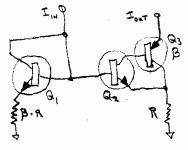
My first shot at an error correcting high magnification current mirror is attached. Q1 and Q2 are matched transistors. Q5 and Q6 are matched transistors. Q3 has a nominal current gain "Beta". Q4 added to increase output impedance. Q2 and Q3 automatically operate with a loop gain to correct about half of any error in output current due to Q3 Beta variation with signal. Q1 and Q2 operate under near identical conditions (coll. current and voltage) so current tracking should be good.
Q5 and Q6 act as an error correction feedback loop (a la Hawksford style error correcting output stage). Q5 and Q6 form a diff. pair to detect remaining output error. Their gain is heavily degenerated by Rdegen resistors so that the inverted error (and error signal only) is fed back into the mirror input as current feedback with just under unity gain. (Load resistors on the diff. pair should be high enough value to look like a current source compared to the low impedance mirror input point.)
Needs a few refinements yet, like a Wilson mirror type input to currect for Q1 and Q2 base currents. Significant point here is that Q3 (well, and Q4) can be a power output transistor with no need for matched high current transistors. Maybe can delete Q4 for an output stage since high output impedance is no big deal in that case. That might affect the accuracy of Q1,Q2 tracking, but again the error correction should fix that too.
Needs some simulation runs now.
Don
Attachments
smoking-amp said:Any mirror designs around that get really large current gains, like 50 or 100?
Don,
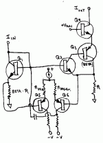
Apart from the error correction, your design of a high ratio current mirror has been practiced befor by Blomley (gain of 1000). An example by Hans Hartsuiker is given below. Note: R22 and R32 should be R56 instead of 56R, i.e. 0.56 Ohm.
Steven
Attachments
Gosh darn it! Somebody already invented it! (Moderator that was a typo, I meant to say "varmit") ")
Thanks Steven, interesting, at least I know its workable now. I think I've even seen that design before and never noticed the significance of Tr1 and Tr5 in it. Nothing new under the sun I guess.
Don
Thanks Steven, interesting, at least I know its workable now. I think I've even seen that design before and never noticed the significance of Tr1 and Tr5 in it. Nothing new under the sun I guess.
Don
Hi,
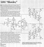
I have seen the 50W "Blomley" posted here before by Steve and I am still pussled what it is really doing even if I understand it... or perhaps should say what is the idea behind it.
But as far as I have studied the circuit with my eyes I feel that the current mirror (alone in this circuit) is not really tracking the current going through TR1 and R20 since the output transistor, when they start to draw current through R22, they offset a bit TR2 working point and this depends also on the output load which use to be a loudspeaker...
..am I missing something here?
Cheers Michael
Hi Michael,
As a first approximation (talking the mirror here) I would think of Tr1 and the combo of Tr2,3,4 as the two transistors in a current mirror. R20 and R22 being the typical emitter resistors to get better tracking (usually R20 shown on the emitter side). In this case Tr2,3,4 has much higher current gain, Beta, than Tr1 so the R20 and R22 are sized in accordance with the currents. Can think of Tr2 operating with a separate emitter resistor equal to that on Tr1, and Tr3,4 having a separate emitter resistor sized smaller for Tr3,4. For emitter resistors sized according to effective Betas (and currents), the emitter resistors would have the same voltage across them. Then can combine Tr2 emitter resistor and Tr3,4 emitter resistor together with no effect to get circuit shown. Thus Tr2 operates under identical current as Tr1 to give current tracking. As Steven pointed out, R22 is .56 Ohm and R20 is 560 Ohm for a 1000 to 1 current ratio which would correspond to Tr2,3,4 having an effective Beta 1000x that of Tr1.
The puzzling resistor is R23. This would seem to cause some mistracking of Tr1 and Tr2 current and hence the overall mirror current gain result. Perhaps it is a tweek added later to compensate for variation of the Tr3,4 group Beta with signal current. Since this design is somewhat sensitive to the Tr3,4 Beta. (Tr2 does try and correct by its emitter follower neg. feedback effect, but maybe only has 100x loop gain) Would have to simulate or measure the actual circuit I guess to see what exactly is going on there.
The small but real sensitivity to output transistor Beta of this design (Tr3 and Tr4 in this case) is the reason I went and added error correction to it a few posts ago as a fix up.
Don
Hi Don,
thanks for your view!
I took a look at the circuit and reread the article a bit more carefully.
They are mentioning that this circuit never is going into class-B operation, they say in the article that the output is always on and here comes the puzzling R22 and R23 in to play as I can see and it's quite clever.
If the output current is decreasing (through R22) then the voltage is increasing over R23 and thereby the mirror trany is feeding the output transistor with more current to keep up and maintain a bias current through the output transistors and thereby no output transistor will go off.
Michael
No, the fact that each output half is never switching off is due to R21 and R31. They cause a small additional current (independent of signal) in the output. Then, this current is the minimum current. The signal part is coming from Tr8 and Tr10. These two are the current separators. If the opamp goes negative Tr8 will sink current but cannot source; if the ouput goes positive then Tr10 will source current, but cannot sink. Tr8 and Tr10 are fast switching small transistors and they can switch much faster then a traditional class B output stage.
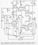
The original Blomley circuit is below.
Steven
The original Blomley circuit is below.
Steven
Attachments
smoking-amp said:Many bipolar transistors have a peaked curve for current gain versus current. One could try to operate in the flat portion (class A) only, but this would restrict operation with severe power inefficiency I think. How about combining MosFet and bipolar some way. If the MosFet transconductance were increasing at the same rate as the bipolar current gain were decreasing (on the high current side of the peak), maybe could get constant transconductance over a fairly wide range? Maybe a Mosfet follower driving a bipolar follower output, class A?
You can try that, but from my experience you can't count on
consistency in the parts, and even when it works you will have
suppressed a low order harmonic and perhaps created more
high order. All told, it's not at all worth the effort unless you
just want to experiment.
Steven,
you are right in that respect the output transistor will never switch off, and I admit I was not accurate in my statemen.
However the point was that there is an active mechanism especially with R22 in the current mirror path.
The R21 is correctly setting a minimum current but it's quite passive due to what's happening at the output.
The R22 in series with the mirror transistor TR2 is affecting TR2 to decrease the bias current when the output current is rising, and increasing the bias current when the output current is approaching zero and thereby giving a softer current overlap (or how i should express it) and this was my point.
Michael
Ultima Thule said:They are mentioning that this circuit never is going into class-B operation, they say in the article that the output is always on and here comes the puzzling R22 and R23 in to play as I can see and it's quite clever.
Are you certain? I look at that circuit and see the output
transistors switching on and off.
This is my confusion also. At what current (ampere, or miliampere), a final stage considered "not-turning off"?Are you certain? I look at that circuit and see the output transistors switching on and off.
ClassA guys maybe will say minimal passing 10mA is equal to OFF condition, no better. Just how much steady bias (in all cycle) for output transistors can be considered "not turning off"?
Nelson Pass said:
Are you certain? I look at that circuit and see the output
transistors switching on and off.
Nelson,
whenever one of you Big guys on this board ask; "Are you certain.." you make one shaking of hes pants...
However, asides from the Hartsuiker circuit, imagine how an output, EF, transistor(in an amplifier circuit) will act if you have a tiny current feeding all time the base.... can it switch of as long as there is a voltage headroom and there is a path for the current to take?
Lumanauw,
when is an output transistor "OFF", technically speaking or what is common thinking in audio community when speaking working classes for output transistor...
For me a transistor is off when Vbe is zero and there is only a leakage Ic current, so even 1uA bias is in my book theoretically class AB...
Cheers Michael
I think there are two issues at hand. One is about the efforts to avoid completely switching off a minority carrier device such as a bipolar transistor. I believe techniques for this has been on the market for quite some time (+25 years) under various "non-switching" names. The second issue is avoiding a discontinuities in the forward gain. This cannot be avoided with "non-switching" techniques since only one half of the stage is actively working with the signal for parts of the cycle. It is the "actively working with the signal" that is the ground for classification in A, B or C, not whether there is some current flowing through the device (or that there is some Vbe). It must be signal related. I think it is important in any discussion to uphold the differences between the grounds for amplifier classification and the consequences of a certain class of operation. We can battle (some of) the consequences of a certain class (such as non-switching class B) but not the class of operation in themselves (it is still class B).
Sincerely,
Kranis
Sincerely,
Kranis
Ultima Thule said:whenever one of you Big guys on this board ask; "Are you certain.." you make one shaking of hes pants...
However, asides from the Hartsuiker circuit, imagine how an output, EF, transistor(in an amplifier circuit) will act if you have a tiny current feeding all time the base.... can it switch of as long as there is a voltage headroom and there is a path for the current to take?
I say "are you certain" because I don't like to be in error, but
looking at the circuit I didn't see how the all output devices would
stay conducting over the operating envelope. This certainly
is not a reproach to the quality of the Bromley circuit.
Certainly it's easy enough to achieve such an effect, and I
invented two of them - one which injects current into the base
of the output all the time, and another which was the one I
patented in 1976. I didn't choose to use the former, but I
noticed later that Technics picked it up in one of their amps.
I didn't use it because like the SAE design, the output devices
remained on, but the signal passed through diodes that did
switch on and off, so you couldn't argue that the signal actually
passed through devices all of which were always forward biased.
Kranis;
By actual definition, Class A is where the gain devices remain
in forward bias all the time, but of course that leaves a lot of
wiggle room for imaginative designers. As a result, additional
descriptive terms have been tacked on, and "pure Class A"
has entered the language to distinguish it from anything which
idles at less than twice the rated output (assuming, of course
that the rated output is the real output).
As a practical matter, when I see a "Class A" amp where the
idle is less than the rated output, I think that the marketing
deparment has taken over.
smoking-amp said:Hi darkfenriz,
True enough, trying to find a large transistor with identical properties to a small one looks unlikely, but how about we make one:
The super matched transistors like the MAT01 ...04 series use an array of identical small transistors with half and half wired in parallel to make two larger transistors. We just need some micro-gremlin to go in there and chop off some connections from one group to get a small one. More likely, a visit to some custom IC Fab place to make a new metalization layer for us.
not, need to simulate:
Here's a tube version of a similar concept:
http://www.tubecad.com/articles_2001/Inv_Dist_Cancellation/index.html
Sheldon
dynamicaly biased class A
Integrated amplifiers are not our favourite, but thay may have cool feature. I think about addind another gang (is it good word?) to the input attenuator. Then simple (or not) circuit could keep bias according to the volume of input signal.
It works good only with standard line level signals, but we are talking DIY. Right? We know whats on the output of our DAC?
I use 20W per channel amp, in a small room with quite efficient speakers. Usually I set my volume knob at 30%. Am I right it would suit it perfectly?
Do you think it's a good idea?
Anyone does it in commercial products?
- Simon
- Status
- This old topic is closed. If you want to reopen this topic, contact a moderator using the "Report Post" button.
- Home
- Amplifiers
- Solid State
- How to cancel odd order harmonics?