
It's still all wrong, you seem to be drawing without any thinking. Driving the primary between OUT_A and OUT_B is neither compatible with AC coupling in the secondary side nor with single gate zeners. Also, you have to figure out why everything is very likely to explode in your last snubber schematic, and which transients are the slower ones and the faster ones with respect to the load current.
eva,
sorry us nebraskans are a bitslow. maybe this is my problem with exploding fets.
i have only delt with thyristor and mercury rectifiers in switching power supplies in the past , they are slower and more forgiving.
i am trying to learn this with more complex solid state stuff.
i have read and played with lower current boost and buck mode and thought i would try the high power stuff.
i guess i need to study more on this area of gate drive.
do you have a working schematic of this area?
do you prefer transformer drive or solid state like IR 2112?
i have found that the ir2112 seems to be sensitive to transients on high current buck.
thank you for your help.
jimbo
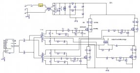
Here you have a couple suggestions...
Transformer gate drive with buffered turn off:
Use fast high current small signal transistors like BC327 or BD140. The 1uF capacitor has to be low ESR and not polar. The diodes may be replaced by Schottkys like 11DQ6.
Full bridge snubbers:
There is a center tap in order to grant symmetric switching, that may help to cancel common-mode EMI depending on how the transformer is wound. By the way, if the bridge is operated properly and the RC across the primary winding provides enough damping to prevent the "second bounce" due to leakage inductance resetting after turn off, then you will no longer need to care about body diodes
Component values are only for reference and have to be tuned to each particular application. RC networks are intended to tame a particular tank circuit resonating at a frequency F, and optimum values usually satisfy the following formula: F=1/(RC) where R is chosen to be the highest value that produces reasonable damping. By the way, I assume that you own an oscilloscope.
Note that SMPS is a bit more critical than 50Hz switching. Concerning IR211x they are fine, I have used them without problem in circuits switching high voltages quite fast, all what they require is careful layout because PCB parasitistics can produce unexpected voltage drops and currents that could blow the IC by exceeding its ratings. Indeed, in SMPS you will discover that everything is full of unexpected voltage drops, currents flowing where they shouldn't and unexpected tank circuits resonating at several Mhz made out of PCB and component parasitistics.
Enjoy")
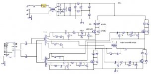
Transformer gate drive with buffered turn off:
An externally hosted image should be here but it was not working when we last tested it.
Use fast high current small signal transistors like BC327 or BD140. The 1uF capacitor has to be low ESR and not polar. The diodes may be replaced by Schottkys like 11DQ6.
Full bridge snubbers:
An externally hosted image should be here but it was not working when we last tested it.
There is a center tap in order to grant symmetric switching, that may help to cancel common-mode EMI depending on how the transformer is wound. By the way, if the bridge is operated properly and the RC across the primary winding provides enough damping to prevent the "second bounce" due to leakage inductance resetting after turn off, then you will no longer need to care about body diodes
Component values are only for reference and have to be tuned to each particular application. RC networks are intended to tame a particular tank circuit resonating at a frequency F, and optimum values usually satisfy the following formula: F=1/(RC) where R is chosen to be the highest value that produces reasonable damping. By the way, I assume that you own an oscilloscope.
Note that SMPS is a bit more critical than 50Hz switching. Concerning IR211x they are fine, I have used them without problem in circuits switching high voltages quite fast, all what they require is careful layout because PCB parasitistics can produce unexpected voltage drops and currents that could blow the IC by exceeding its ratings. Indeed, in SMPS you will discover that everything is full of unexpected voltage drops, currents flowing where they shouldn't and unexpected tank circuits resonating at several Mhz made out of PCB and component parasitistics.
Enjoy
thank you eva
i will try this.
what i am finding out is that the application notes and datsheets as well as much of the other technical literature out there lacks much in the practical detail and application of this area of smps.
i have looked at schematics then at the animal and i see parts added in to apperently solve specific problems.
without this forum i would be very frustrated.
gratefully
jim
jamesrnz said:steve,
thank you for the feed back, enlightening.
i was discussing this with n-channel also he also recommended contiuous mode. so that is where i will go once i ge the full bridge convertor running.
thanks
jimbo
Jimbo, Hint: N-Channel & Steve, they are one-in the same.
Steve, a.k.a. N-Channel
N-Channel said:
Jimbo, Hint: N-Channel & Steve, they are one-in the same.
Steve, a.k.a. N-Channel
I was just checking to see if you were paying attention

sorry
jimbo
gate voltage and logic level mosfets
ok ya'll,
opinions
i have been looking at data sheets and would suggest that some problems with random gate activation could be due to the logic level mosfet that can come on at 2v GS.
since this improvment, gate drive technique is even more important.. since small spikes could easily exceed this level.
jimbo
(please don't beat me too bad)
Eva said:That's true, but your MOSFETs should not be logic level. Have you tried my circuit?
yes i have wired up the circuit in to the bridge,
it looks like it works well with no load, however, i do not have any more fets i will have to order some monday from digikey.
stw20nm50 are what i have been using, aparently they have a gate threshold of 2 volts.
my question was just an observation about logic level fets to see if i was off base.
thanks
jimbo

Usually when one MOSFET turns on too at a too high dV/dt slope the opposite MOSFET also tends to turn on because that slope is coupled back to its gate through drain-gate capacitance. The only two cures are reducing turn-on dV/dt (higher turn-on gate resistor value) and lowering the turn-off gate impedance (pulling down the gate with a heavier buffer). Note that a buffer transistor like the one you are using is already a great improvement over a transformer, and you can reduce the 1K base resistor further to 470 ohms if required.
jamesrnz said:
I was just checking to see if you were paying attention
sorry
jimbo
Uh huh. Must've been those cold Nebraska nights.
Eva, Thanks for the good base drive ckt. I am in the process of diong a 2-ch amp with 2 SG3525s synch'ed, driving small base drive xfmrs, and when I get to that stage of development, I will play around with it.well
i have received a pair of etd59 cores from ferroxcube and a pair of
e71/33/32 e cores both in 3c90.
i am winding the e71's with 5 layers of #22 in 38 turns for the pri.
and 5 turns of .018 copper 1.5 inches wide for the secondary.
2 layers pri, then sec. and three layers of pri.
i just got a variac so i can do variable input voltage up to 120 vac
instead of various transformers.
( this is a full bridge with a doubler input for 320vdc to the fets)
i will put together a schem so far and post it for comments later today.
jimbo
Jimbo,
I have not read this thread too thoroughly so forgive me.
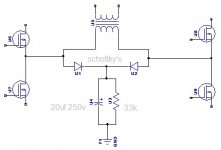
Anyhow I looked at your last schematic, why do you have lots of diodes around all switching FET's??
If the bounce is MORE than the rails voltage of 320 Volts it wont be clamped because your diodes prevent the intrinsinc FET diode to clamp the overshoot.
Also you have more switching losses with these diodes and they cost money, make no sense to me.
Cheers Michael
I have not read this thread too thoroughly so forgive me.
Anyhow I looked at your last schematic, why do you have lots of diodes around all switching FET's??
If the bounce is MORE than the rails voltage of 320 Volts it wont be clamped because your diodes prevent the intrinsinc FET diode to clamp the overshoot.
Also you have more switching losses with these diodes and they cost money, make no sense to me.
Cheers Michael
- Status
- This old topic is closed. If you want to reopen this topic, contact a moderator using the "Report Post" button.
- Home
- Amplifiers
- Power Supplies
- hi power smps