pcb
BV,
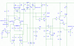
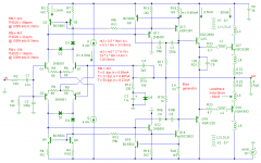
Hereby the pcb print in color pdf. You can clearly see :
BLUE : powerplane mostly (bottom layer BLUE -fourth layer-)
RED & GREEN : signals (top layer RED, second layer GREEN)
WHITE (barely visible) : GND layer - 3rd layer. It actually separates the blue layer from the green & red layer because it is a full plane.
some points :
there are 5 different gnd's they are not connected to eachother on the pcb.
DC GND + is only connected to C1 100nf dc decoupler
DC GND - only to C2 idem
GND IN only connected to 10K Zin R1
GND FB only connected to C4 and D5
GND connected to the gnd plane whitelayer and all other grounds on the pcb not listed here above. that is : collectors q11 q12 and r17 r18
the long red line from is output to vas input is interrupted because i wanted it to be switchable (you can see the funny bridge in my previous photos) so in reality connection is made with bridge
on the right the output of the vas between collectors q14 q15 (cascodes) it is also connected through bridge . it also bridges the line going to the feedback blue going to c6 r15.
I hope you analyse it...
i send pcb and schematic
BV,
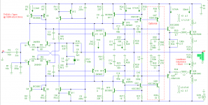
Hereby the pcb print in color pdf. You can clearly see :
BLUE : powerplane mostly (bottom layer BLUE -fourth layer-)
RED & GREEN : signals (top layer RED, second layer GREEN)
WHITE (barely visible) : GND layer - 3rd layer. It actually separates the blue layer from the green & red layer because it is a full plane.
some points :
there are 5 different gnd's they are not connected to eachother on the pcb.
DC GND + is only connected to C1 100nf dc decoupler
DC GND - only to C2 idem
GND IN only connected to 10K Zin R1
GND FB only connected to C4 and D5
GND connected to the gnd plane whitelayer and all other grounds on the pcb not listed here above. that is : collectors q11 q12 and r17 r18
the long red line from is output to vas input is interrupted because i wanted it to be switchable (you can see the funny bridge in my previous photos) so in reality connection is made with bridge
on the right the output of the vas between collectors q14 q15 (cascodes) it is also connected through bridge . it also bridges the line going to the feedback blue going to c6 r15.
I hope you analyse it...
i send pcb and schematic
Attachments
I hope you don't mind me criticicing your pcb layout. 
I'm honest with you:
The amp topology does not require a 4 layer board at all. I think you could do the job with a much cheaper 2 layer board as well.
White as a color for a layer is a bad idea. It's very hard to see on white background. Please do the folks trying to help you a favor and pick another color.
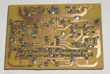
You component placement should be much more dense to reduce parasitic inductance and loop area. You board looks huge (100x160m?). Try to decrease board size.
Drawing connections over components in a schematic looks odd.
You create way too many unnecessary loops. Try to avoid that by using another layer when necessary. Rotate components (e.g. R15) to minimize loop area.
For you input stage current source for example: Place components closer to the heat sink to minimize trace length. Don't take off in the middle of tracks that carry any current. Swap C3 with the diodes to the left, take off at the cap. By the way: What is the current through your input stage? Is it necessary to heatsink Q9 at all? (Sorry, I didn't follow the thread.)
You supply decoupling caps are at the wrong end of the pcb. Charging currents flow through the rail, causing a voltage drop increasing with frequency in the rail tracks. Use a much more massive track, better a plane for your supply rails and place the decoupling caps where you connect wires to the rails. Having a separate decoupling ground as you did is good.
Take more care of grounding. A plane does not magically solve all your grounding. Component placement is more important.
However I don't think the pcb is the reason for you amp running amok. Bad layout can stimulate oscillation and in an amp that isn't stable by itself do a lot of harm. A stable amp should tolerate bad layout to some extent.
The advice I give you is not intended to bash you. Please don't get it wrong. I just share some of my experience of six years doing pcb layout for a living.
Thanks
Lee
I'm honest with you:
The amp topology does not require a 4 layer board at all. I think you could do the job with a much cheaper 2 layer board as well.
White as a color for a layer is a bad idea. It's very hard to see on white background.
Please do the folks trying to help you a favor and pick another color. You component placement should be much more dense to reduce parasitic inductance and loop area. You board looks huge (100x160m?). Try to decrease board size.
Drawing connections over components in a schematic looks odd.
You create way too many unnecessary loops. Try to avoid that by using another layer when necessary. Rotate components (e.g. R15) to minimize loop area.
For you input stage current source for example: Place components closer to the heat sink to minimize trace length. Don't take off in the middle of tracks that carry any current. Swap C3 with the diodes to the left, take off at the cap. By the way: What is the current through your input stage? Is it necessary to heatsink Q9 at all? (Sorry, I didn't follow the thread.)
You supply decoupling caps are at the wrong end of the pcb. Charging currents flow through the rail, causing a voltage drop increasing with frequency in the rail tracks. Use a much more massive track, better a plane for your supply rails and place the decoupling caps where you connect wires to the rails. Having a separate decoupling ground as you did is good.
Take more care of grounding. A plane does not magically solve all your grounding. Component placement is more important.
However I don't think the pcb is the reason for you amp running amok. Bad layout can stimulate oscillation and in an amp that isn't stable by itself do a lot of harm. A stable amp should tolerate bad layout to some extent.
The advice I give you is not intended to bash you. Please don't get it wrong. I just share some of my experience of six years doing pcb layout for a living.
Thanks
Lee
Hi Lee Knatta, no problem to take critics ... If everyone would say : "looking good" I won't get any further now would I?
I chose white because if I use another color you cannot see the blue anymore since it is underneath the white one which in fact is almost a complete GND plane.
About the 4 layers you are right it can be done in 2 but I thought to give me some space and comfort to layout clear tracks without funny twists and turns. Just straight forward close to how it look on the schematic. But it seems that is not a god idea since some tracks are too long now.
The board is indeed around 10cm x 20cm. And there isn't even an OPS No I am not proud!
No Only Q14 and Q15 need heatsinking because they receive the VAS Iq and nearly 60V Vce. This isn't dramatic yet but in the end I want to get my rail power up to 75V or 85V since I want something like 250W into 8ohms. However my PSU only provides 63V max. I did not place the heatsink on the others like Q9.
Q9 is the provider of the tail current and it is around 5 to 6mA.
I need to place the decoupling caps near the place where my powersupply probes get hooked up on the PCB? Indeed they come on the right side whereas the decoupling caps C1 and C2 are on the left side.
About track wideness I guess this will be of consideration when I will build the PCB with OPS. This PCB is only prototype to test IS and VAS so no large currents involved.
I can only ask you to look even deeper in my project (you can find the pcb , schematic, and even pictures of the pcb and pictures of scope traces...) well if you have time off-course ... cause next time I generate a PCB I want it to be right
Just to make you laugh (or shout out loud) my previous attempt to pcb was a 30cm x 40cm pcb with 2,4mm thick FR4 and 70um Cu tracks gold immersed. They cost 350€/piece ! What a waste ...
Could you also check the circuit topology?
See you later...
Olivier
I chose white because if I use another color you cannot see the blue anymore since it is underneath the white one which in fact is almost a complete GND plane.
About the 4 layers you are right it can be done in 2 but I thought to give me some space and comfort to layout clear tracks without funny twists and turns. Just straight forward close to how it look on the schematic. But it seems that is not a god idea since some tracks are too long now.
The board is indeed around 10cm x 20cm. And there isn't even an OPS
No I am not proud!No Only Q14 and Q15 need heatsinking because they receive the VAS Iq and nearly 60V Vce. This isn't dramatic yet but in the end I want to get my rail power up to 75V or 85V since I want something like 250W into 8ohms. However my PSU only provides 63V max. I did not place the heatsink on the others like Q9.
Q9 is the provider of the tail current and it is around 5 to 6mA.
I need to place the decoupling caps near the place where my powersupply probes get hooked up on the PCB? Indeed they come on the right side whereas the decoupling caps C1 and C2 are on the left side.
About track wideness I guess this will be of consideration when I will build the PCB with OPS. This PCB is only prototype to test IS and VAS so no large currents involved.
I can only ask you to look even deeper in my project (you can find the pcb , schematic, and even pictures of the pcb and pictures of scope traces...) well if you have time off-course ... cause next time I generate a PCB I want it to be right
Just to make you laugh (or shout out loud) my previous attempt to pcb was a 30cm x 40cm pcb with 2,4mm thick FR4 and 70um Cu tracks gold immersed. They cost 350€/piece ! What a waste ...
Could you also check the circuit topology?
See you later...
Olivier
Hi Olivier.
I upload the circuit that I use, PCB (hand-made, one side 10x7cm) and capture of simulation.
Build the amplifier on protoboard, more easy to find the error or mistake.
Maybe you must begin to build the amplifier of 0%.

I upload the circuit that I use, PCB (hand-made, one side 10x7cm) and capture of simulation.
Build the amplifier on protoboard, more easy to find the error or mistake.
Maybe you must begin to build the amplifier of 0%.
Attachments
Dear Oliver
During breakfast I quickly read over this thread.
I don't understand much of what is written here. I'm not good at amp design. But what I read is that the amp has conceptual problems and I think your pcb layout is not the main reason for instability. However it is a good idea to improve it.
Forget about the four layer board, use a two layer one. Four layers a waste of money. You already wasted enough money. Most people get away with one layer boards. The ground plane is unnecessary. You have 8 connections to ground, two of them decoupling ground. A star ground will do the job - maybe even better than the plane. My above tips are still valid. Try to reduce trace length and loop area. Loop area also includes attached wires. Your measurement setup might have an influence on the circuit. When doing board layout consider every piece of trace as an inductor. The longer the trace the worse it gets. Just imagine your schematic with dozens of inductors in series with everything! Think about currents flowing and their returns. Having connections crossing on the opposite side of the board is not a problem, just avoid running anything parallel for a longer distance, except things that belong together like differential signals and supplies.
For checking circuit topology I'd need a spice schematic. Which circuit simulator do you use? A LTspice schematic would be nice.
By the way: I need help myself: Please visit my project and leave a comment.
http://www.diyaudio.com/forums/solid-state/164531-another-one-build-av800-av1000.html
During breakfast I quickly read over this thread.
I don't understand much of what is written here. I'm not good at amp design. But what I read is that the amp has conceptual problems and I think your pcb layout is not the main reason for instability. However it is a good idea to improve it.
Forget about the four layer board, use a two layer one. Four layers a waste of money. You already wasted enough money.
Most people get away with one layer boards. The ground plane is unnecessary. You have 8 connections to ground, two of them decoupling ground. A star ground will do the job - maybe even better than the plane. My above tips are still valid. Try to reduce trace length and loop area. Loop area also includes attached wires. Your measurement setup might have an influence on the circuit. When doing board layout consider every piece of trace as an inductor. The longer the trace the worse it gets. Just imagine your schematic with dozens of inductors in series with everything! Think about currents flowing and their returns. Having connections crossing on the opposite side of the board is not a problem, just avoid running anything parallel for a longer distance, except things that belong together like differential signals and supplies. For checking circuit topology I'd need a spice schematic. Which circuit simulator do you use? A LTspice schematic would be nice.
By the way: I need help myself: Please visit my project and leave a comment.
http://www.diyaudio.com/forums/solid-state/164531-another-one-build-av800-av1000.html
... But what I read is that the amp has conceptual problems and I think your pcb layout is not the main reason for instability. However it is a good idea to improve it.
Hmmm perhaps......


Why so insistent on using mirrors to load the input diffs? Do you think using current mirror will affect the sound that much? IHO it doesn’t affect near as much as overcompensation or other slew limiting issues. I would just replace the mirrors with some nice metal film resistors, balance the current in the legs of the input diffs, and call it simplified.
CBS,
I guess it will not affect the sound that much. But lets say I am still naive and a bit a datasheet buff ;-) ... However I am starting to lean towards simplification because I mass murdered already lots of Q's ... Lucky I was never crazy enough to connect the OPS as frying MOSFETS is financially unhealthy
I also see it like a quest
And 3rd I really feel strange to read over and over again that Slone states black on white : This topology is SOO nice because everytime I build it, powering it up is just lovely because everything works 1st time without any wobbles or other funny traces! How is this possible?? My astonishement is accentuated because he often modifies base circuits to get rid of ill defined parameters ... and ultimately the Rolls-Royce circuit is completely ill defined??
"All the trouble I've ever been in started out as fun" ...... RIGHT !!!!!!!
Lee,
I took a quick look at your thread. You use a differential VAS ... I am not very familiar with that topology. I can only say that in slones book it doesn't perform that well... I will take a closer look...
Take a look at the spectrum site MICROCAP they have a demo version. I use that mostly...
For now I must continue working before my boss catches me
Till later....
This conceptual problem was DC conditions instability. It is not problem more (I hope, the last posted schematic is not actual..). What we have to deal with is AC instability. It is not conceptual problem (Nyquist), but implementation (TPC compensation in balanced circuit), PCB layout , parasitic capacitancies in critical nodes (e.g. inverting input and CM outputs in input stage, very long traces, capacitancies against power and GND layers) and and inductancies (long, thin traces), and maybe components used (MJE340/350 in VAS).
It will be best solution to build this circuit on protoboard first, with lower DC rails. And then redesign PCB (2 layers more than enough) )and with respecting to some rules.
It will be best solution to build this circuit on protoboard first, with lower DC rails. And then redesign PCB (2 layers more than enough) )and with respecting to some rules.
Last edited:
BV,
Yes the last posted schematic is the one that corresponds with the PCB layout in order for you to understand track layout.
I will dispose of it in the end. It will become like your modification or simply with resistor loads in the diff amp IS.
The components used are not really MJE340/350 (they are the best I find in the simulation library) but 2SD669 and 2SD649. Because my stock of them is running out I could only find NTE373 & NTE374 devices which should be near 2SB and 2SD...
By the way do you have good alternative?
About protoboarding. I imagine a protoboard really be a mess with bridges and thick solders, etc... how could this be better than a real tracked PCB? Even if the PCB is not well layed out... Or am i wrong about this?
I got another question, does anyone know how to match transistors ?
I have only a scope 40Mhz , psu 2x60V(3A), multimeter True RMS DC+AC, function generator 10Mhz and a low cost multimeter containing a HFE measurement.
The HFE measurement is lousy i think and by the way it doesn't measure Vbe differences between Q's.
Do I have to setup a circuit?
Buy equipement ??
I have only a scope 40Mhz , psu 2x60V(3A), multimeter True RMS DC+AC, function generator 10Mhz and a low cost multimeter containing a HFE measurement.
The HFE measurement is lousy i think and by the way it doesn't measure Vbe differences between Q's.
Do I have to setup a circuit?
Buy equipement ??
New try
Good evening everyone!
I would like to thank all of you for all the replies and valueble information!
I will give my amplifier project a new try. I will use the same topology but with this change : I will follow BV's approach. I modified the schematic accordingly. The schematic is added here in pdf format.
This time I count on all you guys help to critisize my progress ! That way I will correct the problems before I irreversable decisions are made
I will go through this project step by step and give feedback every step of the way, so afterwards some of you can do the project without going through the trouble...
Hope you guys agree and support me...
I plan to work in different steps :
1) making the base schematic (this done)
2A) putting it on DIY for your remarks (done - waiting for replies)
2B) be critical on myself since tomorrow may reveal better ways
3) Put the schematic into simulator to finetune components choice
4) Open discussion about results etc. with you on DIY
5) Discuss component types what Q's? Cap types? Res types? Diodes...
6) Finalize schematic and shop for components
7) Create base pcb
8) Place it on DIY for your remarks
9) Finalize pcb layout
10) manufacture pcb
11) solder pcb
12) testing
13) discussing findings & conclusions
14) integrate OPS etc ... but this is for much later
Did I forget something?
Now step 1 is done, step2 :
- What are the first impressions of the schematic?
- Question : R17 and R18 serve to bias the zeners. Originallly they were both connected to the GND, but is this necessary or better to do it? Or can it be bound together without reference to the ground? Slone does it for R12 which biasses the diodes D1,2,3&4. Same counts for R17,18? The reason for leaving it with 2 resistors instead of one is because of the heat. Remember I will later use 75 to 85 V rail supply! Goal is between 250 & 350W into 8 ohms.
- Question : I lately see often cascoded input stages. Is this useful? What is the benefit?
-Question : is two pole compensation a good thing or not?
- Question : What about the feedforward circuit R14, C6? It is typically a Slone approach...
- R24,25 : Are used for measuring VAS Iq and should later on be used as current limitting sensors for protection transistors in the VAS leg.
- R26 is a 10K load which I could place or not while testing.
- Rout is a resistor I placed on BV's proposition to coop with probable scopeprobe capacitance problem.
- The collectors of Q11 and Q12 are connected to ground. Could I also connect them together and leave a gnd reference out of it? I am affraid they are not matched (Q11,Q12) and therefore the connection node will not be at 0V but e.g. +4Vdc which in return could cause less swing? Right or Wrong?
Your turn guys
Attachments
Good evening everyone!
[snip]
Did I forget something?
Now step 1 is done, step2 :
- What are the first impressions of the schematic?
Nice try, but frankly speaking, it could be better.
- Question : R17 and R18 serve to bias the zeners. Originally they were both connected to the GND, but is this necessary or better to do it? Or can it be bound together without reference to the ground? Slone does it for R12 which biases the diodes D1,2,3&4. Same counts for R17,18? The reason for leaving it with 2 resistors instead of one is because of the heat. Remember I will later use 75 to 85 V rail supply! Goal is between 250 & 350W into 8 ohms.
It's better to do it your way. Avoid unnecessary connections to gnd, in particular if it is a signal gnd.
- Question : I lately see often cascoded input stages. Is this useful? What is the benefit?
Not that much. It only makes sense if you strive for ultra low distortion (below 1ppm). But then a simple cascode is not enough; use Hawksford cascodes instead. In that case however, you will get other problems: it's not only more complicated but also prone to HF oscillations.
-Question : is two pole compensation a good thing or not?
It's bad, because of overshoot and unnecessary loading of the VAS. Use TMC instead, i.e. tie (my) R24/25 to the output instead of gnd.
- Question : What about the feedforward circuit R14, C6? It is typically a Slone approach...
It's just optional. Generally, just for compensation of parasitic capacitances. See C8 in my schematic.
- R24,25 : Are used for measuring VAS Iq and should later on be used as current limiting sensors for protection transistors in the VAS leg.
That's okay. To be on the safe side is not a bad idea anyway.
- The collectors of Q11 and Q12 are connected to ground. Could I also connect them together and leave a gnd reference out of it?
No!
I am afraid they are not matched (Q11,Q12) and therefore the connection node will not be at 0V but e.g. +4Vdc which in return could cause less swing? Right or Wrong?
Due to mismatches one of the trannies will certainly go into saturation. But that's not all. The collector voltages should held constant in order to avoid a Miller effect from Cob.
Your turn guys
Okay, my turn.
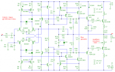
Below you see another approach how to define and stabilize the VAS current.
The inputs of the VASes are connected via 10k resistors (R18/20) to the bases of the current sources, which act as a temperature compensated reference (more or less).
At 27 dgrs. Ic = 8.4mA, increasing to 9.5mA at 0 dgr. and decreasing to 7.5mA at 50 dgrs.
By varying R12/13 you can tailor Ic according to your needs.
BTW, notice that the tail currents are also a bit temperature dependent.
As there's no feedback action between the emitters of the VAS and the current mirrors, the gain is much higher and accordingly the distortion much lower.
I've omitted the VAS cascodes as they hardly improve the performance. Probably because of the outstanding properties of the KSA1381 and KSC3503 (and of course due to the preceding emitter followers Q15/16)
Cheers,
E.
Attachments
What Mr Slone neglected to do
Hi guys,
One more example how to tame the VAS standing current. This one is based on BV's idea, i.e. local feedback around the VAS and current mirror. Consequently, it doesn't rely on the specifics of the tail currents sources as in my previous example. So you are free to choose any CCS you like.
In order to ease manipulation of the local loop gain, the VASes have their own emitter resistors (R19,20). Next, the emitter resistors of the current mirrors are chosen such that the voltage drop across them is the same as across R19,20 (see the formulas in the schematic)
Now we can put a feedback resistor of any value between the emitter of Q5 and Q13 (respectively Q6 and Q14) without disturbing the DC operation point.
In the final version I've put the FB resistors between the base of Q5 and Q13 (respectively the base of Q6 and Q14), as (for some reason) I got 6dB more loop gain at the same level of distortion.
There is a trade-off between DC stability and distortion: the lower Rfb the more stability AND the more distortion. So, what's the optimal value of Rfb? Hard to say, but at least we need a reasonable amount of (local) NFB, say 20dB. This means Rfb~=4k7. With this value the distortion is about 6dB higher than the lowest you can get, so it's not that bad a compromise.
Cheers,
E.
Attachments
Hello,
Thanks for your first replies Edmond Stuart ! I put my schematic in the SPICE simulation now and will let you know the results. As for your 2 variants to tame the VAS Iq I will study them too...
Where are the rest of you guys? Everyone agrees with Edmond Stuart
Edmond, when you say ppm its part per million? so 18ppm = 0,0018% ?
When you say the GAIN of the VAS reduces due to the LFB between VAS and IS ... how much is that? And I don't see exactly why ... Can you show it in a formula?
thnx
Hi guys,
I simulated all day. Just a lousy rainy day as usual in Belgium, we are used to that
As you all know I started with a 100% Slone topology. The one that has an ill defined VAS Iq. Indeed its not working. Many have tried to find solutions to stabilize Iq. From what I simulated on the Slone circuit I got at best 0,0004% or 0,4ppm or 400u% of THD at 1kHz 50Vpp. The proof of being unuseable for me was the fact that if you do a sensitivity test on the CM left degeneration resistor the Iq in the VAS's dependency was 133 !!!!!!!!!!!!!!!!!!!!!!!!!
To make it work I implemented a modification Mr. BV offered. I simulated a THD of around 0,0012% or 1,2ppm or 1,2m% of THD. 3x times worse. But the VAS IQ was stable. The same sensitivity test showed 1,6 instead of 133.
Now I tried an own modification where the sensitivity is about 20. The THD is even better than Slone base circuit however I must say it might be possible I didn't optimize that circuit well enough to compare...
The THD is 0,0002% or 0,2ppm or 200u% at 20KHz 50Vpp. @1KHz 50Vpp it is : 0.00024% or 0,24ppm whic is worse than at 20KHz How comes?? At 50KHz it rises tot 0,004% or 4ppm.
Remember there is no OPS yet and the stage was loaded with 10MOhm
What did I do? Instead of creating a LFB around the vas legs and the right IS CM degen resistor I left the vas legs connected to the rail as the base circuit but i did bv's mod with the darlington Q legs. I then used a smal resistor in the vas legs to sense changes .... pff difficult to explain look at schematic, its better
I like the thd results and when R2 changes + or -1% the vas Iq changes from 17mA over 22mA to 27mA. Whereas slones circuit causes the same change of R2 to move the Iq from 0.1mA over 30mA to 63mA -> a 630x change ! mine changes only 1.6x !
You guys like it or did i overlook the basics here and i will go down in flames
by the way hereby sensitivity results :
I(R22)
Name Value Sensitivity Sensitivity (%/%)
R2.Value 75 -0.00618999 22.6831
R3.Value 22 0.0164162 -17.646
R4.Value 22 0.0164222 -17.6524
R6A.Value 2.2 0.0157768 -1.69587
R5.Value 75 -0.00591974 21.6927
R6B.Value 68 0.00627205 -20.8386
R7.Value 22 -0.0165536 17.7937
attached :
schematic
schematic with currents
bode
THD
Attachments
Hello,
Thanks for your first replies Edmond Stuart ! I put my schematic in the SPICE simulation now and will let you know the results. As for your 2 variants to tame the VAS Iq I will study them too...
Where are the rest of you guys? Everyone agrees with Edmond Stuart
Edmond, when you say ppm its part per million? so 18ppm = 0,0018% ?
Yes, it is. For low distortion figures I favor ppm over %. So 1ppm instead of 0.0001%.
I hate to count all those ****** zero's.
When you say the GAIN of the VAS reduces due to the LFB between VAS and IS ... how much is that? And I don't see exactly why ... Can you show it in a formula?
thnx
The VAS input current is amplified by beta, causing a voltage across R15 (and R16), which is fed back as current via Rfb to the current mirror. So the FB factor (or local loop gain) is approximately beta * R15 / Rfb
If beta =100, Rfb = 4k7 and R15 = 2k2, then LG ~= 130*2.2/4.7 ~= 47 (33dB)
Notice that this local loop gain comes at the expense of the overall loop gain, hence more distortion.
Cheers,
E.
Distortion is quite high Edmond at 14ppm. I would think you should be getting <10ppm 100W 20KHz into 8 Ohms with this sort of topology. How would you reduce it further and do you think its actually worthwhile (other than the intellectual challenge)?
Hi Bonsai,
Sure, it can be made better at the cost of more components (no free lunch
 )
)See below.
Hi guys,
.........
You guys like it or did i overlook the basics here and i will go down in flames
.........
THD
Hi Olivier,
I'm afraid you do. Sorry. Although you did improve the sensitivity WRT resistor values, you're still not done yet. The problem is that the VAS Iq also relies on perfect matching of the IPS and CM trannies.
I think the only way to get rid of this is a common mode control loop (CMCL) that directly monitors Iq and keep it under tight control.
Below you see two versions: a simple one that needs four additional trannies (Q13...Q16) and a slightly better one that needs six extra trannies (plus Q27, Q28).
The 2nd version makes use of a copy of the VASes. The collector currents of these copies are summed together(as voltage across R40/41) and this 'sum' is fed back to the current mirrors (via Q15/16). Q14 and Q15 provide a reference current in order to balance the circuit. When using this version omit C11/12; R22/23; R25/26 and tie the collectors of Q19/20 to gnd.
The 1st version senses the VAS Iq indirectly by monitoring the collector currents of emitter followers (Q19/20). Although it does work, it's not that accurate, as Iq also depends on Vbe matching of emitter followers.
The unity loop gain frequency of the CMCL is set by C11/12 & R22/23, i.e. 360kHz (or C18/19 & R42/43 for the 2nd version, i.e. 590kHz). This ULG frequency is not critical, but take care of sufficient phase margin, preferable >= 90 degrees.
Cheers,
E.
PS: In case the VASes show some oscillations you might try C9 = C10 = 100pF.
BTW, 'Ed' is an abbreviation of 'Edward'......
Attachments
- Status
- This old topic is closed. If you want to reopen this topic, contact a moderator using the "Report Post" button.
- Home
- Amplifiers
- Solid State
- HEEEELLLPPP : M. Randy Slone Mirror Image Topology Construction - Troubles