No, watch again the schematics, this is not luck.Stable VAS?
Just beginners luck, the worst that can happen to you.

There is no buffer transistor in VAS, Q29 don´t work very high Iq.
Furthermore, R36 help to "stabilize" the stage.
Put 2 transistor or beta enhancer, and the first transistor (buffer) like 2N3904 or BC547 maybe it will be destroy, or become very very hot.
Hi Edmond! When I build this amplifier on protoboard, I use VAS like page 247 (Douglas).
No cascode. 2 transistor put very hot (Q28 and "his symetric") in VAS.
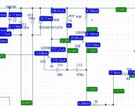
I add a capture from PSPice.
Iq = 9.140mA, Vce = 22V - 1.152V = 20.84V, Pdis = 0.19W
datasheet from BC547, Rth(c-a) = 83ºC/W => Tc = (15,7 + 25)ºC = 40.7ºC (in theory)
I upload files in another replay, the circuit for PSPice is a .rar file.
Of course I am not an expert and I appreciate any sugestion, the amplifier works well, but I can upgrade! (i.e. DC servo)

No cascode. 2 transistor put very hot (Q28 and "his symetric") in VAS.
I add a capture from PSPice.
Iq = 9.140mA, Vce = 22V - 1.152V = 20.84V, Pdis = 0.19W
datasheet from BC547, Rth(c-a) = 83ºC/W => Tc = (15,7 + 25)ºC = 40.7ºC (in theory)
I upload files in another replay, the circuit for PSPice is a .rar file.
Of course I am not an expert and I appreciate any sugestion, the amplifier works well, but I can upgrade! (i.e. DC servo)
Attachments
Can you guys tell me something about one of my previous questions?
I agree that the Slone schematic as we speak is ill defined and it puts the VAS either in Class C or in BBQ mode. Even if by luck it has an Iq of say 20mA it would run away through temperature changes bringing us back to Class or BBQ anyway.
I often encountered both of the situations and sometimes even a working one.
But what I also get very often is RF Oscillation !? Has that anything to do with the ill defined Iq in the VAS? Directly? Indirectly?
I am quite sure it is not Nyquist problem, I don't think Ground loop problems and I guess not RF pick-up by air.
My RF situation show up in two forms. Sometimes I get an ugly sinus but periodic fix frequency but the frequency is not every day the same. Sometimes 100kHz sometimes 300kHz sometimes 1Mhz. The other form of RF is more a very ugly signal non periodic but with periodic large spikes. I can also tell i sometimes have a very high freq sinus of 30Mhz but this is very low voltage (500mV) where the other two problems i mentionned show almost rail to rail voltages.
The only thing I can think of , is that the ill DC problem inherent on the schematic causes the powersupply to run into protection mode (constant current) which then lowers the rail voltage of one side. This lock in lock out condition continiously glitches and gets the amp in a 'nowhere' situation causing the power supply to go quickly IN and OUT of protection like tak-tak-tak-tak-tak ... (When I hear that sound I feel like throwing it out of the window") )
)
Anybody some good reply?
I agree that the Slone schematic as we speak is ill defined and it puts the VAS either in Class C or in BBQ mode. Even if by luck it has an Iq of say 20mA it would run away through temperature changes bringing us back to Class or BBQ anyway.
I often encountered both of the situations and sometimes even a working one.
But what I also get very often is RF Oscillation !? Has that anything to do with the ill defined Iq in the VAS? Directly? Indirectly?
I am quite sure it is not Nyquist problem, I don't think Ground loop problems and I guess not RF pick-up by air.
My RF situation show up in two forms. Sometimes I get an ugly sinus but periodic fix frequency but the frequency is not every day the same. Sometimes 100kHz sometimes 300kHz sometimes 1Mhz. The other form of RF is more a very ugly signal non periodic but with periodic large spikes. I can also tell i sometimes have a very high freq sinus of 30Mhz but this is very low voltage (500mV) where the other two problems i mentionned show almost rail to rail voltages.
The only thing I can think of , is that the ill DC problem inherent on the schematic causes the powersupply to run into protection mode (constant current) which then lowers the rail voltage of one side. This lock in lock out condition continiously glitches and gets the amp in a 'nowhere' situation causing the power supply to go quickly IN and OUT of protection like tak-tak-tak-tak-tak ... (When I hear that sound I feel like throwing it out of the window
)Anybody some good reply?
guys,
I simulated a 4th schematc now (after the slone based, the bv based mod and the one using resistive coll load in the cm) i tried the one of havenwood. slone based but without the darlinton or beta enchancer. i did'nt fiddle too much with the other components yet so it is probably not optimal but if one changes too much values the comparison is also a bit lost... so first impressions are :
Iq vas seems now less sensitive to comp tol% (compared to slone) but more than in bv's or resistive load topology.
thd is around 0.0045% just better than resistive load but worse than all others
AC analyses seems odd. it must be nyquist unstable ... funny how the phase shift flies towards 180° on a fast rate while gain is slowers so at -180° still 10db gain???
i dont know why but there seems to be a zero in the plot forcing the gain to rolloff too slowly
any comments?
Hawenwood´s schematic is using TPC (two pole compensation) with (IMO) a little strange values. So slope of LG decline is steeper. With balanced input and VAS configuration it is much more prone to unstability (both halves are not 100% symetrical..) And TPC is always causing overshoots.
Last edited:
I ran across a curiousity while browsing through slones book. Looking at figure 11.12 and 11.14 they are both the configuration we discuss here in this thread (MI:mirror image, BE:beta enhanced, CC:cascoded vas, CM:current mirror).
Slone always uses a current limiter in the VAS through the use of a resisive sensor driving a protection transistor.
In figure 11.12 this value is 33ohms and in 11.14 it is 4.7ohms?
If we expect the VAS to be at 60% of protection value in both cases ->
Iq VAS 11.12 would be : 11mA
Iq VAS 11.14 would be : 77mA
What is the purpose of this large difference? And how comes this large difference?
BV circuit in practice
Today I wanted to try BV's modification to Slones circuit (the one I made and call 'Base Circuit' in this thread). Here is my report :
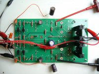
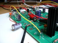
Attached is a picture of the base topology PCB as tested.
File : Base Circuit.jpg
File : Base.pdf for schematic
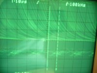
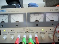
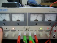
First I powered up the base. It went into instant barbeque mode pushing the power supply into protection, power supply goes click-clack-click-clack etc. Hereby attached a picture of the scope trace while click-clacking. And also attached a picture of the power supply unit showing red leds on -> protection mode notice voltage flyback. The right PS is green and red at the same time showing it is clicking into and out of protection fast.
File : Scope Base Circuit.jpg
File : Crazy PSU.jpg
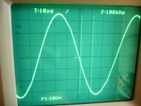
Just for testing I added to R2 on the base schematic a parallel resistor of 1Kohm. This causes the left upper current mirror degenaration resistor to drop from 75ohms to 70ohms. What happenend? The VAS goes from BBQ mode to Class C mode. There isn't any VAS Iq left. In the simultation the VAS Iq should have been 35mA with all CM degeneration resistors at 75ohms. In reality it must have been much more like 1 or 2 amps (that is BBQ mode). When in simulation you reduce the resistor R2 from 75 to 70 the Iq VAS becomes just nano amperes which corresponds to Class C.
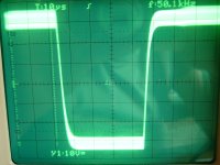
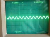
I attached a scope trace of the class C operation. Look at the little edges on the sinus.
File : Scope Class C.jpg
Next I implemented BV's modification. See attached schematic and PCB picture. On the picture you can see the yellow wire from emitter Q16 to resistor split on the right CM (picture taken on neg rail side but is same on positive side)
File : BV.pdf
File : BV.jpg
When I powered up I was happy. I got a full 60V + and - without any protection issues. Circuit stabilized immediately. Iq VAS measured 10mA where it was simulated for 6 to 7mA. But thats not a problem.
See Power supply picture :
File BV PSU.jpg
Everything was stable and AC was OK. But I had 570pF as miller caps implemented (i did that to make sure to stay out of nyquist problems and to isolate other problems). So I reduced them first to 47pF. This was not stable as I got quite some noise on the trace. I then upped the miller to 100pF which I find OK (it would give you about 50 to 60V / us which is fast enough for a 250 to 300W Power Amp).
Then I put a square wave on the input causing a 60Vpp swing on the output. There is no overshoot and slew rate measured around 50V/us. It would be perfect BUT it is clearly visible there is noise on the trace superposed on the signal. I attached 3 traces : 1) the output square wave 2) same trace but no input signal and scope settings changed to view noise
Well the noise seems to be a pretty sinus looking good 8Vpp swing and 12MHz... Nyquist Oscillator??
File : trace 1.jpg
File : trace 2.jpg
The simulation shows a nice 40 degrees phase margin. Why do i run into this problem?? Is the PCB bad? Are the fltying wires causing this?
I dunno. But it seems my phase shift is larger than in the simulation?
Hope this is usefull for you guys
Anyone can tell me more of my problem,?
Greetz
Today I wanted to try BV's modification to Slones circuit (the one I made and call 'Base Circuit' in this thread). Here is my report :
Attached is a picture of the base topology PCB as tested.
File : Base Circuit.jpg
File : Base.pdf for schematic
First I powered up the base. It went into instant barbeque mode pushing the power supply into protection, power supply goes click-clack-click-clack etc. Hereby attached a picture of the scope trace while click-clacking. And also attached a picture of the power supply unit showing red leds on -> protection mode notice voltage flyback. The right PS is green and red at the same time showing it is clicking into and out of protection fast.
File : Scope Base Circuit.jpg
File : Crazy PSU.jpg
Just for testing I added to R2 on the base schematic a parallel resistor of 1Kohm. This causes the left upper current mirror degenaration resistor to drop from 75ohms to 70ohms. What happenend? The VAS goes from BBQ mode to Class C mode. There isn't any VAS Iq left. In the simultation the VAS Iq should have been 35mA with all CM degeneration resistors at 75ohms. In reality it must have been much more like 1 or 2 amps (that is BBQ mode). When in simulation you reduce the resistor R2 from 75 to 70 the Iq VAS becomes just nano amperes which corresponds to Class C.
I attached a scope trace of the class C operation. Look at the little edges on the sinus.
File : Scope Class C.jpg
Next I implemented BV's modification. See attached schematic and PCB picture. On the picture you can see the yellow wire from emitter Q16 to resistor split on the right CM (picture taken on neg rail side but is same on positive side)
File : BV.pdf
File : BV.jpg
When I powered up I was happy. I got a full 60V + and - without any protection issues. Circuit stabilized immediately. Iq VAS measured 10mA where it was simulated for 6 to 7mA. But thats not a problem.
See Power supply picture :
File BV PSU.jpg
Everything was stable and AC was OK. But I had 570pF as miller caps implemented (i did that to make sure to stay out of nyquist problems and to isolate other problems). So I reduced them first to 47pF. This was not stable as I got quite some noise on the trace. I then upped the miller to 100pF which I find OK (it would give you about 50 to 60V / us which is fast enough for a 250 to 300W Power Amp).
Then I put a square wave on the input causing a 60Vpp swing on the output. There is no overshoot and slew rate measured around 50V/us. It would be perfect BUT it is clearly visible there is noise on the trace superposed on the signal. I attached 3 traces : 1) the output square wave 2) same trace but no input signal and scope settings changed to view noise
Well the noise seems to be a pretty sinus looking good 8Vpp swing and 12MHz... Nyquist Oscillator??
File : trace 1.jpg
File : trace 2.jpg
The simulation shows a nice 40 degrees phase margin. Why do i run into this problem?? Is the PCB bad? Are the fltying wires causing this?
I dunno. But it seems my phase shift is larger than in the simulation?
Hope this is usefull for you guys
Anyone can tell me more of my problem,?
Greetz
Attachments
-
 Base Circuit.JPG539.6 KB · Views: 623
 -
Base.pdf15.6 KB · Views: 158
-
 Scope Base Circuit.JPG498.7 KB · Views: 586
 -
 Scope Class C.JPG499 KB · Views: 547
 -
BV.pdf15.5 KB · Views: 167
-
 BV.JPG520.8 KB · Views: 535
 -
 BV PSU.JPG501.3 KB · Views: 164
 -
 Crazy PSU.JPG492.8 KB · Views: 127
 -
 Trace 1.JPG542.8 KB · Views: 133
 -
 Trace 2.JPG529.9 KB · Views: 133
BV,
Let me know your findings of my last post.
I did still a lot of simulation on your VAS stabilization.
I always came out THD is twice the value of the base circuit.
Now I reduced Vin to half and come out the same THD as the base (slone) circuit. Could it be that large signal is affected by topology? Maybe VAS Iq is in class AB and once signal is large there is a passage from A to B which penalizes the THD score. Is this possible or am I talking sh*t.
Will continue to do testing
So long
Olivier
Let me know your findings of my last post.
I did still a lot of simulation on your VAS stabilization.
I always came out THD is twice the value of the base circuit.
Now I reduced Vin to half and come out the same THD as the base (slone) circuit. Could it be that large signal is affected by topology? Maybe VAS Iq is in class AB and once signal is large there is a passage from A to B which penalizes the THD score. Is this possible or am I talking sh*t
.Will continue to do testing
So long
Olivier
Olivier 73,
AC performance, stability and THD figures are very,very dependant on PCB topology and circuit realisation, grounding scheme and blocking capacitors placing . I see in Your pictures a lot of long wires (in legs of blocking capacitors too,) in air over PCB (big inductance, parasitic coupling in other parts ), thin PCB traces (parasitic inductance). It all has big impact on stability and performance. It seems it is not only input and VAS, but whole amp (transistors with small heathsinks, i dont know schematic).If so, i cannot see any Boucherot cell and output inductor.
Circuit with local feedback to CM is now DC stable, but at the same time you lost some gain in overall feedback, so circuit linearity may be slightly worse compared to original, simulated circuit. But it is reliable working, oposite to original circuit.And yes, linearity is amplitude dependant, so lower THD with lower amplitude (less overall NFB for linearization, so more visible). VAS is workinng iin class A with currents about 10mA, current swing is much less than bias current , so here are no excursions to AB.
Last edited:
Bv,
It is not the whole amp, it is only the IS & VAS. The 2 Q's on the heatsink are the Cascode Q's in the VAS. Since i use 60V rails and Iq was around 60mA in the Slone circuit (for the few times it was stable) they become very hot. 3-4 Watts dissipation.
The picture you saw was the circuit as I last used with Slone topology then I changed the PCB to your modification (yellow wires) on another picture.
The PCB tracks arent that small they must be 3mm wide with a 35um thickness.
The two 470uF blocking caps I removed, they do nothing. The 2 orange ones forms the real blocking caps they are 100nF 250V caps and they have no wires on the rail side. The ground side is linked together with a black wire which in turn runs back to the center tap of PSU with a black clamp and black/red wire.
On the left the funny looking towering components is an input conditionning circuit which I removed because I believe it will be only usefull when final. That was connecter with a red clamp to the function gen. Now it is linked directly to input DC coupled.
Underneath that input circuit you see 2 black clamps. One is NEG of Generator and one goes back to the center tap of PSU.
In the middle you see a large cap (fb dc block cap) a red clamp (out of blacks) goes back to the center tap of PSU and one is NEG of Scope probe.
On the right you see the scope probe signal clamp.
There is another GND red clamp on the right going back to the center tap of PSU. It is gnd that returns Zener ref voltage and collectors of beta enhancers in circuit (Q11&Q12).
The component numbers correspond mostly like the schematic I sent in previous post. The one file with BV.pdf i believe.
To avoid GND and RF problems I tried something radical. The PCB you see is 4 layer PCB.
Bottom is V+ and V- only.
One up is complete GND plane (the one connected with the red clamp on the right of the pcb the one setting zener ref gnd and collectors of Q11&Q12)
2 Top layers is signal layers.
Do you think my problem is RF pickup or GND loop ? Or is it impossible to guess / know? Or do you think it might stil be Nyquist (phase margin).
There is one thing that bothers me on the pcb however. I believe the most sensitive link is the one linking IS output to VAS input. Is that right?
Well, it also is one of the longest tracks. And I find it not well placed. You can see it on the PCB. You will see a soldering bridge on the track which I wanted to be switchable but it is very unelegant... On the one of the bottom(NEG side) you can see it between R9 and R11 if you follow that track it leads you under components like D4, C5, C8, Z2, R21 etc... It runs close to V- rail. I believed it was no problem because between V- track and Singal track there is complete GND plane. But this is off-course not true where components have pass through holes. So it runs close (3mm) to the components pins which are connected to PSU rails.
Do I really have to Redesign another PCB??? This one is the 3rd ... first was crap, second was 350€/pc 30x40cm 2,4mm thick with 70um tracks and I had to trash it because after soldering/desouldering 100 times tracks came off... Grrr was trying to build Slone Amp ! This one has large pads and without OPS and a lot less expansive approx 10x20cm ...
I must rest ...
Too many coffees today
Too many oscillations

However since BV mod no more BBQing components...
It is not the whole amp, it is only the IS & VAS. The 2 Q's on the heatsink are the Cascode Q's in the VAS. Since i use 60V rails and Iq was around 60mA in the Slone circuit (for the few times it was stable) they become very hot. 3-4 Watts dissipation.
The picture you saw was the circuit as I last used with Slone topology then I changed the PCB to your modification (yellow wires) on another picture.
The PCB tracks arent that small they must be 3mm wide with a 35um thickness.
The two 470uF blocking caps I removed, they do nothing. The 2 orange ones forms the real blocking caps they are 100nF 250V caps and they have no wires on the rail side. The ground side is linked together with a black wire which in turn runs back to the center tap of PSU with a black clamp and black/red wire.
On the left the funny looking towering components is an input conditionning circuit which I removed because I believe it will be only usefull when final. That was connecter with a red clamp to the function gen. Now it is linked directly to input DC coupled.
Underneath that input circuit you see 2 black clamps. One is NEG of Generator and one goes back to the center tap of PSU.
In the middle you see a large cap (fb dc block cap) a red clamp (out of blacks
) goes back to the center tap of PSU and one is NEG of Scope probe.On the right you see the scope probe signal clamp.
There is another GND red clamp on the right going back to the center tap of PSU. It is gnd that returns Zener ref voltage and collectors of beta enhancers in circuit (Q11&Q12).
The component numbers correspond mostly like the schematic I sent in previous post. The one file with BV.pdf i believe.
To avoid GND and RF problems I tried something radical. The PCB you see is 4 layer PCB.
Bottom is V+ and V- only.
One up is complete GND plane (the one connected with the red clamp on the right of the pcb the one setting zener ref gnd and collectors of Q11&Q12)
2 Top layers is signal layers.
Do you think my problem is RF pickup or GND loop ? Or is it impossible to guess / know? Or do you think it might stil be Nyquist (phase margin).
There is one thing that bothers me on the pcb however. I believe the most sensitive link is the one linking IS output to VAS input. Is that right?
Well, it also is one of the longest tracks. And I find it not well placed. You can see it on the PCB. You will see a soldering bridge on the track which I wanted to be switchable but it is very unelegant... On the one of the bottom(NEG side) you can see it between R9 and R11 if you follow that track it leads you under components like D4, C5, C8, Z2, R21 etc... It runs close to V- rail. I believed it was no problem because between V- track and Singal track there is complete GND plane. But this is off-course not true where components have pass through holes. So it runs close (3mm) to the components pins which are connected to PSU rails.
Do I really have to Redesign another PCB???
This one is the 3rd ... first was crap, second was 350€/pc 30x40cm 2,4mm thick with 70um tracks and I had to trash it because after soldering/desouldering 100 times tracks came off... Grrr was trying to build Slone Amp ! This one has large pads and without OPS and a lot less expansive approx 10x20cm ...I must rest ...
Too many coffees today
Too many oscillations
However since BV mod no more BBQing components...
Havenwood,
Well it is not really a prototype, at least it wasn't when I started the idea. I used a cookbook design of Slone and voilà I choose a topology that doesn't seem to work. How lucky can you be!?
However I always believed the problem was AC not DC. I thought, on a protoboard with flying wires it will be a mess. My thought were strengthened by the fact that even on a PCB where the RF, GND and other AC things are at least a bit better then on a protoboard it still generated AC problems. However the problem seems to be a combination but mostly DC or at least AC cannot get resolved without DC being OK.
So now I winded up with a 3rd revision of PCB board modified to fit BV's schematic (see earlier postings).
But still, according to myself and BV confirmed there is still an AC problem so the PCB is noot good enough... however I find it hard to believe that I have a nearly 2Vpp 13MHz sinus trace without input signal. And when input is applied it is summed to the 13MHz signal. See also trace in earlier posting.
I use 100pF miller caps and even with 330pF millers it is still there however the amplitude reduces to 500mVpp instead of 2Vpp... Nyquist instability seems not possible for me.
That leaves only a few possibilities :
1) generator or PSU is not quality
2) RF pick-up inductive or capacitive
3) GND loop problems
Damn I feel rotten about this because I don't have enough dep knowledge of audio electronics ...
Havenwood, did you check my posting with pictures yet? Can you take a look and tell your findings?
Olivier
Havenwood,
It will be MOSFET OPS in the end but for the PCB you see is just input stage + VA stage. There is no OP stage yet.
Components are fine, there are no goofs in the nodes, nor broken tracks nor shorted track nor inverted components... in other words the pcb and circuit are electrically OK.
It start to believe that electricity and electronics is the basis but everything what comes after that is ART !
I am not a good artist
Olivier,
instabilty can be caused by capacitive loading, too. Maybe scope probe input capacity can be reason, insert about 100R resistor before probe.
And outputs from CM to VAS transistors should be as short as possible, they are the most sensitive nodes in whole amp for disturbance injection and coupling from suplly rails. But try to post PCB picture, it is most likely reason.
Last edited:
BV,
I will upload pcb asap when i come home this evening.
However how can i do it? 4 different PDF's one for each layer? The PCB is 4 layer.
I noticed something strange while testing yesterday about the probe indeed. I usually keep the probe connected all the time. It happened that circuit worked well except for the little 13MHz 2Vpp oscillation. However when i removed the probe the powersupply went into protection. This means removing the probe causes some important effect !? Cap as you say?
I also always have the problem with my portable multimeter.
To measure Iq VAS there are two 10 ohms resistors between the collector of amplifier Q and emitter cascode Q (slone uses these later for Iq vas protection sensor). Well, when i connect one pin of the multimeter I see funny scope traces RF. Not a nice oscillation but rubbish and very unclear.
Sometimes the power supplie also goes into protection. until i leave the pin off again...
Is that strong sensibility normal?
I will send PCB toninght !
See you later
- Status
- This old topic is closed. If you want to reopen this topic, contact a moderator using the "Report Post" button.
- Home
- Amplifiers
- Solid State
- HEEEELLLPPP : M. Randy Slone Mirror Image Topology Construction - Troubles