take your time and don't rush
read F5 tutorial thread(s) , take a good look on numerous amp pics and think why something is arranged as is
Zen, thank you
") Pretty much what I have done the past month while waiting for parts to arrive
Pretty much what I have done the past month while waiting for parts to arrive  The P3 thing was however an impulse thing
 P1 and P2 are all set to 0 ohm btw prior to soldering them to the board.
Next big assembly will be the PSU, hope the caps arrive soon...
@Rewind - Tjena
Looking forward to see photos Decided on cabinet yet?removing P3 from the amplifier changes the bias current of the amplifier.From last nite I learned P3 is not of same value as P1/2 and since I did not have proper variable resistor on hand I removed P3 from the circuit. I also lifted R7/R8 off the board a little to improve airflow.
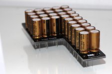
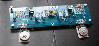
Both boards now populated after tonite session with the iron, only a few vacant locations while I wait for the remaining components to arrive. Soldering went rather well as I am not used to solder small stuff
You should have replaced P3 with some fixed value resistors to maintain the same bias currents.
removing P3 from the amplifier changes the bias current of the amplifier.
You should have replaced P3 with some fixed value resistors to maintain the same bias currents.
I was under the impression that P3 was optional, as in left open ?
I was under the impression that P3 was optional, as in left open ?
exactly
just one thing - whatever you do with part values (already having functional amp) , always reset drain trimpots to zero and repeat setting procedure
First PSU board populated with caps which finally arrived in the mail
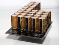
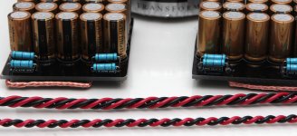
Board is 4mm acrylic with self made vinyl print screen. The images show first PSU bank, the other half will be a mirror image of this one allowing the toroid to fit between the slim PSU ends. Hope it works out good
Board is 4mm acrylic with self made vinyl print screen. The images show first PSU bank, the other half will be a mirror image of this one allowing the toroid to fit between the slim PSU ends. Hope it works out good
Attachments
Thank you I am properly enjoying this build!
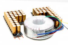
Late sunday nite I wanted to perform capacitance test for the PSU's, part of my desire with this build is to learn more about electronics. Since both cap banks now were completed I wanted to 1) verify proper function and 2) compare the two.
I deviced a setup rig consisting of the DVM, a 10k resistor and a 3-15,5VDC switch mode power supply. Powered it up at V(min) and slowly ramping up to V(max).
The 10k resistor was placed in series with the positive DVM-probe and voltage was read from the display asap the power was cut. Both cap banks were tested individually in order to compare them for discharge/time.
Result:
Time(s) - Vpos - Vneg
0 - 15,39 - 15,40
5 - 10,90 - 11,20
20 - 5,5 - 5,8
30 - 3,3 - 3,6
40 - 2,11 - 2,24
50 - 1,40 - 1,44
60 - 0,88 - 0,92
70 - 0,57 - 0,60
80 - 0,37 - 0,39
90 - 0,24 - 0,26
100 - 0,16 - 0,17
110 - 0,10 - 0,12
120 - 0,07 -0,08
130 - 0,05 - 0,06
140 - 0,03 - 0,04
150 - 0,03 - 0,03
160 - 0,02 - 0,02
Test ended
I am properly enjoying this build!Late sunday nite I wanted to perform capacitance test for the PSU's, part of my desire with this build is to learn more about electronics. Since both cap banks now were completed I wanted to 1) verify proper function and 2) compare the two.
I deviced a setup rig consisting of the DVM, a 10k resistor and a 3-15,5VDC switch mode power supply. Powered it up at V(min) and slowly ramping up to V(max).
The 10k resistor was placed in series with the positive DVM-probe and voltage was read from the display asap the power was cut. Both cap banks were tested individually in order to compare them for discharge/time.
Result:
Time(s) - Vpos - Vneg
0 - 15,39 - 15,40
5 - 10,90 - 11,20
20 - 5,5 - 5,8
30 - 3,3 - 3,6
40 - 2,11 - 2,24
50 - 1,40 - 1,44
60 - 0,88 - 0,92
70 - 0,57 - 0,60
80 - 0,37 - 0,39
90 - 0,24 - 0,26
100 - 0,16 - 0,17
110 - 0,10 - 0,12
120 - 0,07 -0,08
130 - 0,05 - 0,06
140 - 0,03 - 0,04
150 - 0,03 - 0,03
160 - 0,02 - 0,02
Test ended
Last edited:
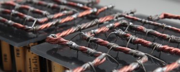
Those thick cables between the Cs avoid the little bit of R between the capacitors and replace it with a miniscule r that has almost no filter effect.
Those thick cables between the Cs prevent twisting of the cabel to attenaute emitted interference.
Using thin wires that are twisted between each C gain twice over in better filtering and better interference attenuation.
Those thick cables between the Cs prevent twisting of the cabel to attenaute emitted interference.
Using thin wires that are twisted between each C gain twice over in better filtering and better interference attenuation.
Image update from Tuesday:
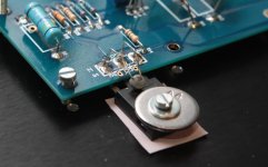
MOSFETs and transistors arrived (Q3-Q6) and I was eager to get on with the build. Drilled 10 perfectly spaced holes with 3mm drill bit only to find out that this was too wide for M3 tapping.. Did a few new ones using a 2.5mm bit and had much better success funnily enough
Mounted the PCB and MOSFET/trans's and soldered them to the board along with the 4k7 thermistors.
MOSFETs and transistors arrived (Q3-Q6) and I was eager to get on with the build. Drilled 10 perfectly spaced holes with 3mm drill bit only to find out that this was too wide for M3 tapping..
Did a few new ones using a 2.5mm bit and had much better success funnily enough Mounted the PCB and MOSFET/trans's and soldered them to the board along with the 4k7 thermistors.
Attachments
anyway , web search is always there , so no need to remember
Indeed, but that is fruitless if one forget to search or assume knowledge

Googlzheimers...
up to 8mm there is a rule - multiply screw metric value by 0.8 and you have drill size
so , for 3mm that would be 2.4mm
anyway , web search is always there , so no need to remember
cool! I never knew that
- Status
- This old topic is closed. If you want to reopen this topic, contact a moderator using the "Report Post" button.
- Home
- Amplifiers
- Pass Labs
- Halair's F5 build