Hi People ")
Long story short, I built myself a pair of fullrange line arrays this spring (my first diy speaker project) and since I know very little about electronics the obvious next step would be to make my own amp
I am curious of class A amplification, the NP F5 is well documented, low part count so seemed to be a good place to start
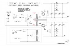
Currently aquiring the necessary parts and waiting for delivery on most of the little stuff. Transformer is a 400VA/2x18VAC toroid and cabinet is a 4U/400mm unit from Modushop.biz in Italy. Both are in house. PCB bought from DiyAudio Store, transistors from h_a and JFET's from Spencer, rest is pretty much via ebay.
My main intent for this thread is to share my experience and seek information/a little guidance along the way I have read a lot in here including the how-to\s provided by L6L and others and it is sinking in
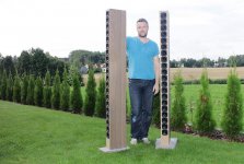
The speakers intended for this amp is a 20driver full range line array with nom. imp=6.4ohm. Calculated 98dB sensitivity => should work ok?
Long story short, I built myself a pair of fullrange line arrays this spring (my first diy speaker project) and since I know very little about electronics the obvious next step would be to make my own amp
I am curious of class A amplification, the NP F5 is well documented, low part count so seemed to be a good place to start
Currently aquiring the necessary parts and waiting for delivery on most of the little stuff. Transformer is a 400VA/2x18VAC toroid and cabinet is a 4U/400mm unit from Modushop.biz in Italy. Both are in house. PCB bought from DiyAudio Store, transistors from h_a and JFET's from Spencer, rest is pretty much via ebay.
My main intent for this thread is to share my experience and seek information/a little guidance along the way
I have read a lot in here including the how-to\s provided by L6L and others and it is sinking in The speakers intended for this amp is a 20driver full range line array with nom. imp=6.4ohm. Calculated 98dB sensitivity => should work ok?
Attachments
.....
The speakers intended for this amp is a 20driver full range line array with nom. imp=6.4ohm. Calculated 98dB sensitivity => should work ok?
naah .......
sissy speakers .......

Vix, thanks Fugly? Naaaah....
My impression of my arrays are that they are very articulated yet go surprisingly low, something I hope the F5 can continue to do. I have no idea what to expect but believe in having as little as possible in the signal path present. The arrays have no filters etc, only analoge EQ to counter the top/bottom rolloff inherent to arrays in general.
ZM, thank you too Hope to pick your brain later once the build progress
Fugly? Naaaah.... My impression of my arrays are that they are very articulated yet go surprisingly low, something I hope the F5 can continue to do. I have no idea what to expect but believe in having as little as possible in the signal path present. The arrays have no filters etc, only analoge EQ to counter the top/bottom rolloff inherent to arrays in general.
ZM, thank you too
Hope to pick your brain later once the build progress Array build log here - http://www.diyaudio.com/forums/full...column-my-line-array-build-20-fr-drivers.html
Have I got this right?
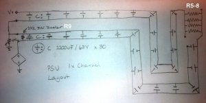
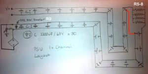
Drawing show layout v1 for physical placement of one channel PSU, I am using 30pcs 2200uF/63V per side, 15 in front of and 15 after R5-8.
I have not correctly drawn rectifier negative to connect with PSU negative rail btw
Toroid will occupy the bottom left side of the layout hence the "heavy" PSU right side.
Attachments
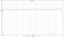
This impedanse plot is from another similar build, same drivers/sealed volume so...fwiw
I havent measured mine.
http://www.rsr-concepts.com/diyma/impedance tests right.jpg
I havent measured mine.
http://www.rsr-concepts.com/diyma/impedance tests right.jpg
The +ve supply and the -ve supply from the rectifier should connect to the same end of the string of capacitors.
The +ve and -ve output from the string of capacitors should come from the same end. i.e. the opposite end from the rectifier connections.
Do not take the rectifier to the Ground and do not take the output end to the Ground.
Maintain the Charging Circuit as it's own CIRCUIT through out. In at one end, out at the other end and low loop area for the whole length of the string.
I recommend that you arrange a time delayed bypass for the NTC.
Otherwise the resistance of the NTC and thus the voltage on the supply rails will change with music volume.
The +ve supply and the -ve supply from the rectifier should connect to the same end of the string of capacitors.
The +ve and -ve output from the string of capacitors should come from the same end. i.e. the opposite end from the rectifier connections.
Do not take the rectifier to the Ground and do not take the output end to the Ground.
Maintain the Charging Circuit as it's own CIRCUIT through out. In at one end, out at the other end and low loop area for the whole length of the string.
Thank you Andrew for adding in, do the revised drawing look more in line with your suggestion?
Attachments
Almost.
You are using the NTC as a slow charge current limier.
It needs to be moved into the charging circuit.
Are you going to adopt the delayed bypass?
I use a 555 as the timer.
It can be set to any time delay from ½second to 60seconds by changing just the capacitor (a cheap MKT or reformed electro).
You are using the NTC as a slow charge current limier.
It needs to be moved into the charging circuit.
Are you going to adopt the delayed bypass?
I use a 555 as the timer.
It can be set to any time delay from ½second to 60seconds by changing just the capacitor (a cheap MKT or reformed electro).
Ok, so the thermistor (NTC) is better placed after the cap bank as per NP schematic, not next after the rectifier as drawn by me?
I am not against a bypass circuit, timed or otherwise, I just haven't spent time investigating it yet as I have wrapped my head around the PSU itself since I am making my own board. My electrical knowledge is limited so my thinking was "stick with what works" and adjust from there. The road to a finished amp is part of this excersise
I am not against a bypass circuit, timed or otherwise, I just haven't spent time investigating it yet as I have wrapped my head around the PSU itself since I am making my own board. My electrical knowledge is limited so my thinking was "stick with what works" and adjust from there. The road to a finished amp is part of this excersise
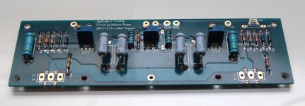
Finally started the actual work for this build
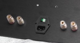
Drilled out the rear chassis panel and inserted IEC block and speaker terminals. Waiting for the RCA before I can complete it.
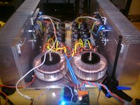
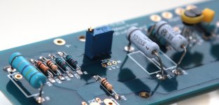
Applied heat to the PCB, started to populate the first board and managed to solder most of one channel Still a couple of key components missing.
Drilled out the rear chassis panel and inserted IEC block and speaker terminals. Waiting for the RCA before I can complete it.
Applied heat to the PCB, started to populate the first board and managed to solder most of one channel
Still a couple of key components missing.Attachments
Last edited:
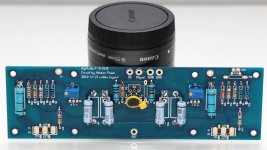
From last nite I learned P3 is not of same value as P1/2 and since I did not have proper variable resistor on hand I removed P3 from the circuit. I also lifted R7/R8 off the board a little to improve airflow.
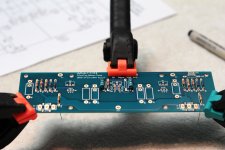
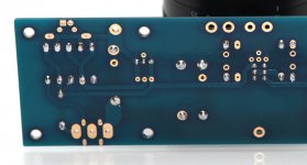
Both boards now populated after tonite session with the iron, only a few vacant locations while I wait for the remaining components to arrive. Soldering went rather well as I am not used to solder small stuff
Both boards now populated after tonite session with the iron, only a few vacant locations while I wait for the remaining components to arrive. Soldering went rather well as I am not used to solder small stuff
Attachments
- Status
- This old topic is closed. If you want to reopen this topic, contact a moderator using the "Report Post" button.
- Home
- Amplifiers
- Pass Labs
- Halair's F5 build